Gas Cluster Beam system UltraTrimmer Plus™/ Acrevia™
Leading trimming technology to bring significant contribution to quality improvement of RF devices
Accelerating growth of mobile networks for smart society by leading-edge smartphones, intelligent cars and innumerable connected IoT devices is expanding the business opportunities for frequency control devices which consist of a number of RF filters. As the cellular market moves to higher frequencies, sensitive control is highly required to meet 4G as well as pre-5G and 5G deployment needs. An energetic, directional, chemical Gas Cluster Beam (GCB) is used for trimming process to control device parameters of RF filters, MEMS, photonic devices, and other various applications. TEL’s UltraTrimmer series provides precise control of film thickness by reducing surface roughness. Cutting edge technology enables industry leading performance: sub-nanometer thickness control, a wide range of dynamic correction and high-throughput processing. UltraTrimmer series realizes a variety of custom process profiles for silicon or compound substrate and contributes to yield improvement and performance enhancement.
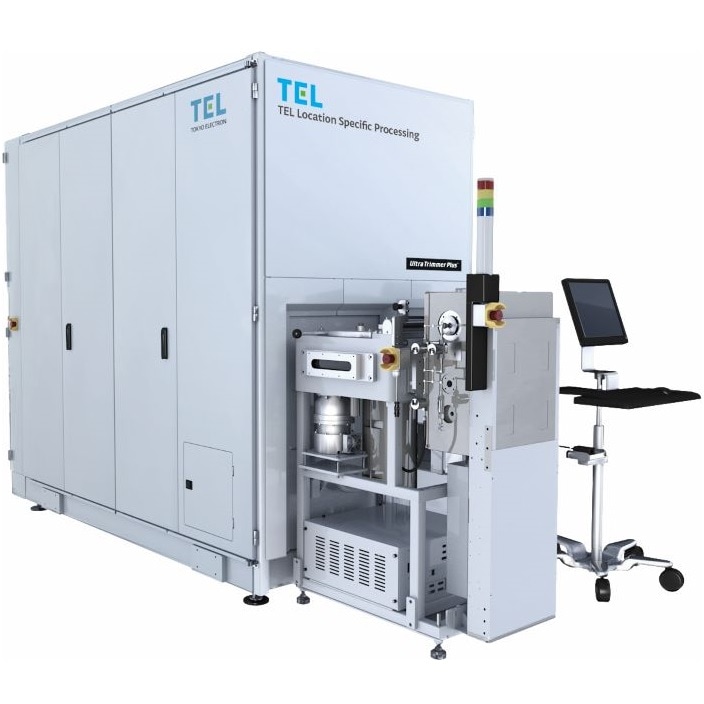
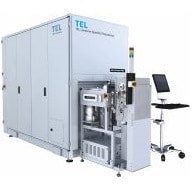
UltraTrimmer Plus™ brings unique trimming technology for 100/150/200mm wafer with industry leading corrective etch capabilities and best in class cost of ownership. To provide higher yield manufacturing, UltraTrimmer Plus™ proposes the most effective solution to reduce various material properties. Its corrective etch enables significant quality improvement of critical layers. Incorporating high accuracy X-Y stage wafer scanning system and newly developed LSP software into APC, through using wafer level metrology data, the system enables film surface planarization and improves etch depth profile of deep trench and hole. Without any hardware changes, the system can handle variety of wafer sizes seamlessly. UltraTrimmer Plus™ provides various applications such as frequency trimming of SAW, BAW and FBAR filters, film surface smoothing of MEMS devices or other timing devices through mechanical and chemical mass etch.
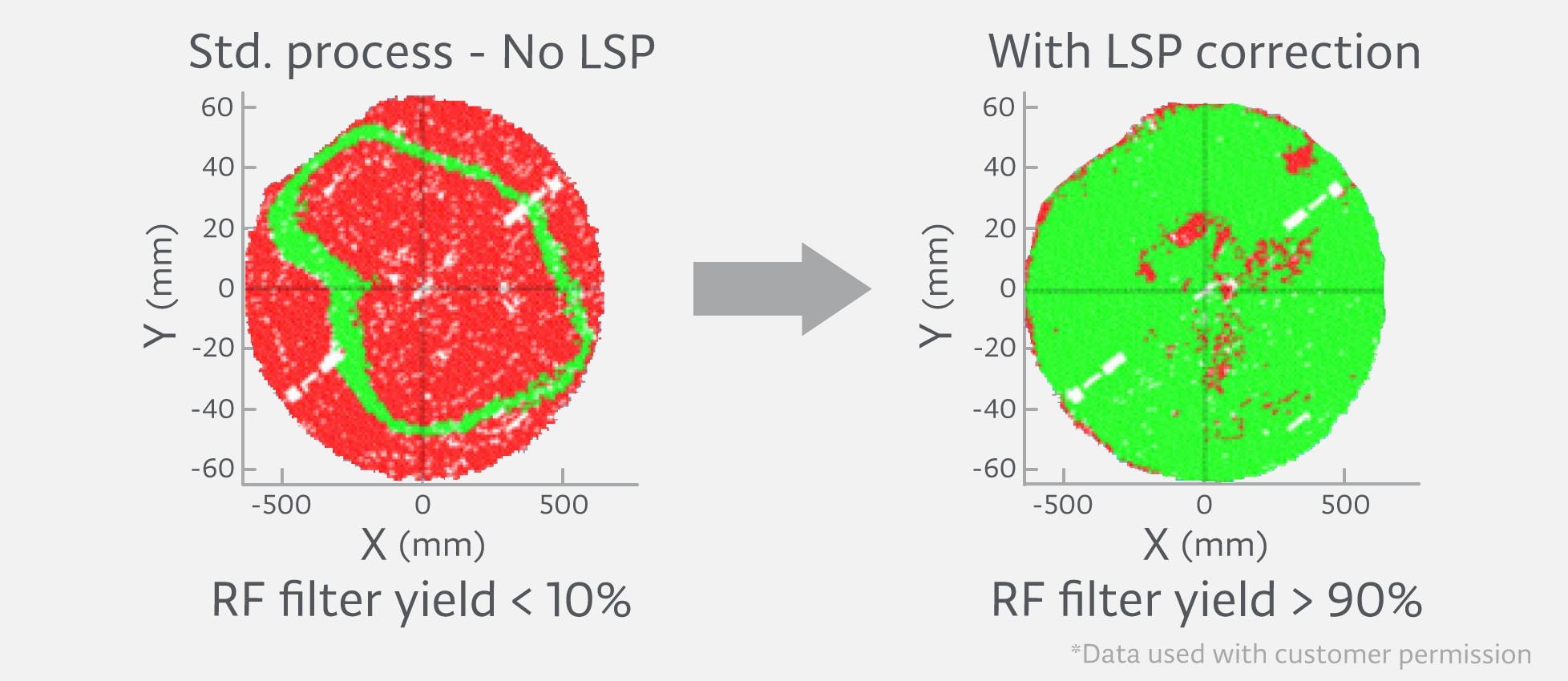
Customer yield map: Devices at target frequency (1)
Customer yield map: Devices at target frequency (2)
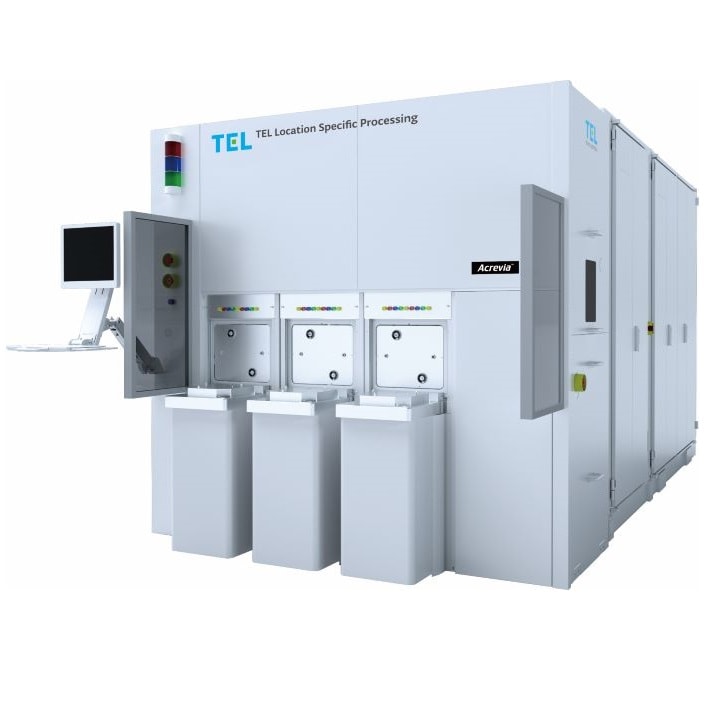
Acrevia™ is a 300mm wafer process tool with a unique etching function that not only reduces the non-uniformity of the wafer surface, but also enables individual control of the etching amount within the wafer. Combining a Gas Cluster Beam (GCB) with a highly accurate tiltable wafer scanning system, it enables flexible and precise correction by corrective etching within the same wafer surface. By applying this technology to processes that previously required multiple EUV steps, it contributes to reducing the number of required steps. Additionally, the use of TEL's proprietary LSP software (Location Specific Processing) ensures superior uniformity control, allowing Acrevia™ to compensate for non-uniform profiles introduced by other processing steps. In addition, it is possible to improve LER (Line Edge Roughness) and reduce lithography defects that cause yield loss.
Product comparison
 |
 |
|
| Wafer size (mm) |
100,150,200 | 300 |
| Availability | New | New |
| Process | Gas Cluster Beam | Gas Cluster Beam |
| Performance | 1σ thickness variation <1nm | N/A |
| Applications | Etching(Frequency trimming, Thickness trimming), Film Conversion(Oxidation, Nitridation), Film smoothing …etc. |
Dimension Modification, WIW Uniformity Control, LER/LWR improvement |
| Features | High throughput and low CoO, Corrective etching (Location specific processing), Room temperature process(No damage, Charging) |
Proven Gas Cluster Beam (GCB) technology for low damage etching, Wafer scanning system featuring wafer tilting to etch feature sidewalls, Location Specific Processing (LSP) algorithm to improve within wafer uniformity |
UltraTrimmer Plus and Acrevia are registered trademarks or trademarks of Tokyo Electron Group in Japan and/or other countries.
