Deposition TELINDY™ Series
State of the art 300mm batch furnace with over 10,000 systems shipped

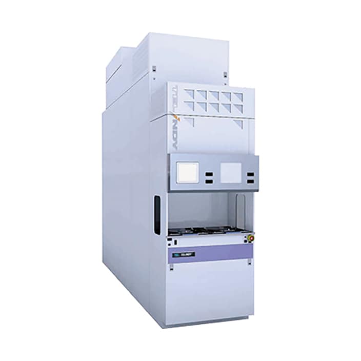
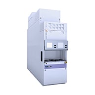
TELINDY PLUS™ is the industry’s premier iso-thermal large batch platform for oxidation, anneal and LPCVD deposition which are at the core of semiconductor manufacturing. TELINDY PLUS™ incorporates the pinnacle of hot wall reactor technology and enables superb film quality while maintaining the ultimate in process control and run to run stability. Additionally, TELINDY PLUS™ is designed with all of the essential architectural design features which maximizes wafer throughput per square foot. Since its introduction, TELINDY PLUS™ has continued to evolve in capability featuring increased wafer batch sizes and expanded process applications for low temperature ALD (Atomic Layer Deposition) and plasma assisted deposition (TELINDY PLUS™ IRad™) required by ever shrinking device structures, thus supporting the leading edge in device manufacturing.
TELINDY PLUS™ represents the convergence of demonstrated experience and leading edge thermal processing technology. TELINDY PLUS™ incorporates specialized features originally developed for short TAT (Turn Around Time) on the TELFORMULA™ minibatch system as well as field proven, high productivity design elements from the previous generation TELINDY™ platform. Process performance and productivity have continued to improve and further expanded to ALD applications. New enhancements include improved maintenance access through architectural optimization to further reduce maintenance down time. Dry gas chamber cleaning and low O2 environment loading area control have realized tangible gains in small particle management contributing to yield increases. The highest levels of productivity have been achieved by combining 125 wafer load size with TEL’s FTPS™ responsive heater capable of rapid heating and cooling coupled with a dual boat system option. TELINDY PLUS™ applications range from traditional silicon treatments such as diffused oxides and anneals to LPCVD Si (Poly Si, a-Si), SiO2, Si3N4 to leading edge ALD SiO2, Si3N4 and high-k dielectrics as well as radical (non-plasma) oxidation.
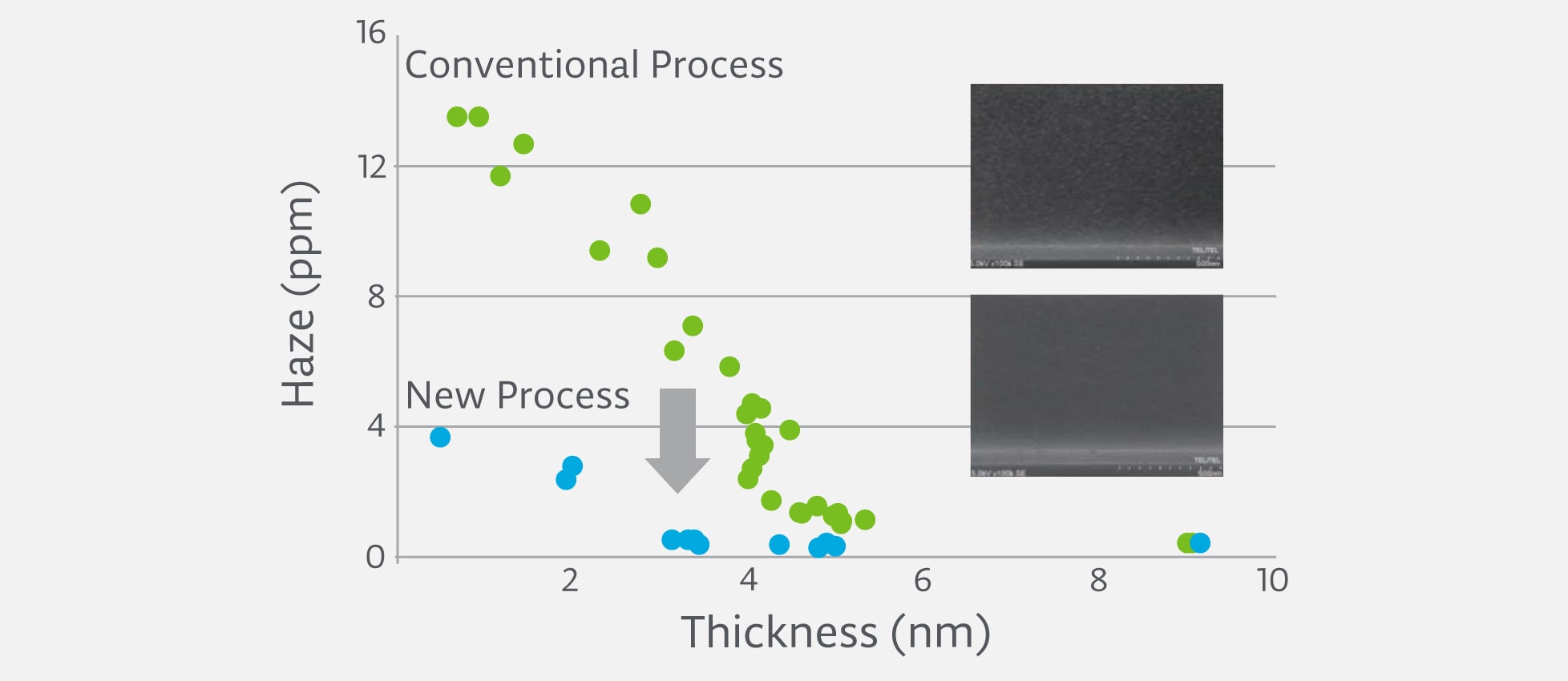
CVD Si surface morpgology
TELINDY PLUS™ IRad™ is the definitive intersection between thermal large-batch and plasma processing. TELINDY PLUS™ IRad™ maintains all of the design advantages of the field proven, high productivity and reliable TELINDY PLUS™ platform while incorporating a damage-free plasma capability. Thus, the TELINDY PLUS™ IRad™ further extends the process domain of batch technology to new, lower temperature regimes while maintaining deposited film quality. TELINDY PLUS™ IRad™ provides a stable platform for high quality thin film deposition at low temperature which is increasingly desired for advanced device scaling and dense 3D structures. Predominant applications include ultra-low temperature ALD Si3N4 and SiO2. With the included dry gas cleaning capability, both down time reduction and superior particle performance are realized.
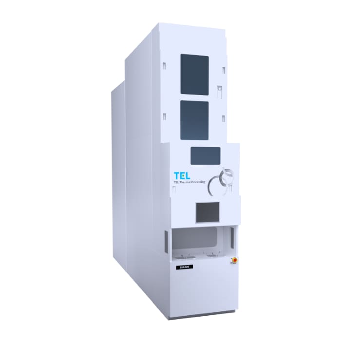
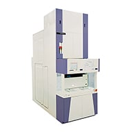
EVAROS™ processes up to 200 wafers (300 mm) per batch—the highest capacity compared with previous models. Together with reduced wafer transfer time, it delivers very high productivity.
The thermal control system, a key element of any batch thermal processing tool, uses a newly developed multi‑zone control heater with improved dynamic response, achieving excellent temperature uniformity and significantly shortening temperature ramp and stabilization times. Enlarged exhaust piping improves conductance, enabling high‑precision, high‑quality film control for ALD processes and other requirements of high‑end devices.
From an environmental perspective, EVAROS™ reduces power, cooling‑water and gas usage, achieving approximately 25% lower CO2 emissions per wafer compared with TELINDY PLUS™.
Also, an automatic position‑adjustment function for the wafer handler shortens installation time and reduces maintenance effort. A next‑generation, expandable system controller supports autonomous operation in the future by enabling the addition of diverse functions*.
Current applications include ALD SiO2, ALD SiN, and Poly; subsequent additional applications include high-k and more.
*smart tool matching, health monitoring etc.
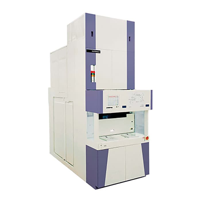
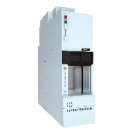
TELFORMULA™ is the semiconductor industry’s most advanced iso-thermal minibatch platform. TELFORMULA™ incorporates a number of innovative technologies specifically developed to address the industry’s need for a 300mm high speed batch platform capable of delivering short TAT (Turn Around Time) both suitable for product development and simultaneously capable of meeting demanding, high-volume production requirements. The short TAT is achieved by the convergence of multiple new core technologies, such as a metal-free fast ramping heater, low thermal mass chamber, rapid gas volume purge/displacement and a high speed wafer handling unit. The all quartz reactor concept provides the ideal processing environment for attaining the ultimate level of cleanness which is maintained by in-situ chamber dry gas cleaning reducing maintenance downtime and related costs. TELFORMULA™ is the ideal platform for a wide variety of semiconductor processes including LPCVD Si (Poly, a-Si), Si3N4, SiO2, ALD High-k, ATM/LP Oxidation, Oxynitridation, etc.
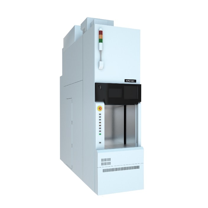
ALPHA-8SE™ i is a vertical batch thermal processing system for 200mm wafers. Released in 2018 by remodeling its predecessor ALPHA-8SE™ under the three concepts of innovation, inherit, and evolution, ALPHA-8SE™ i has received high acclaim for its stability and productivity.
Innovation
As more than two decades have passed since the release of ALPHA-8SE™, some of its parts are likely to be discontinued in the near future. In the renewed model, those parts have been replaced to enable the latest system configuration, while parts interchangeability with 300mm vertical furnaces was secured to achieve greater operational stability and continuity.
Inherit
The proven process performance of the ALPHA-8SE™ series continues to be available together with a wide variety of upgrade kits. The system can process 150/200mm wafers in a batch of up to 150, and is suitable for diverse applications including oxidation/annealing, chemical vapor deposition (CVD) of Si (Poly, a-Si), SiN, and SiO2 films, and atomic layer deposition (ALD) of high-k films.
Evolution
A number of improvements and enhancements have been incorporated in the renewed model. To reduce the burden of daily inspections, for instance, more system parameters are now captured and displayed on the control panel, which are also made accessible to our data collection system (Ingenio™) and customers to reinforce the system’s remote monitoring capability. An auto logout feature has been added to the control panel, preventing inadvertent work interruptions and input errors. The adoption of an exhaust pipe heater for efficient warming and decreased outgassing improves the system’s functionality and ease of operation. Conformity with international safety standards including SEMI S2*and CE marking**means the system shares the same specifications throughout the world and can be offered in any region.
* SEMI S2: An environmental, health, and safety guideline for semiconductor production equipment. It has been adopted by leading semiconductor device manufacturers in the U.S. and Europe, and also serves as a safety guideline of manufacturing equipment for electrical and electronic devices throughout the world.
** CE marking: Products exported to be sold in the European Economic Area must conform to relevant EU directives, and are required to carry CE marks that certify their safety.
Product comparison
 |
 |
 |
 |
 |
|
| Wafer size (mm) |
300 | 300 | 300 | 300 | 150, 200 |
| Availability | New | New, Certified used | New | New | New |
| Production load max | -200 | -125 | -50 | -125 | -150 |
| Cassette stocker | -22 | -18 | -10 | -18 | -21 |
| Process | Oxide, Nitride, Poly | Thermal ALD, LPCVD, Oxididation/Anneal |
Oxide, Anneal, Nitride, Poly, TEOS, High-k |
Plasma Assisted ALD SiN, SiO2* |
Oxide, Anneal, Nitride, Poly, TEOS, HTO, High-K |
| Reactor | Thermal | Thermal | Thermal | Plasma | Thermal |
| Process temp | RT-800C | RT-1100C | RT-1000C | RT-800C | RT-1250C |
| Additional features, Option | N2/LL Gas cleaning |
N2/LL Gas cleaning |
N2/LL Gas cleaning |
N2/LL Gas cleaning *RT SiO2 |
N2,/LL, Gas cleaning: CIF3 for poly |
TELINDY, TELINDY PLUS, EVAROS, TELFORMULA, IRad, FTPS, and ALPHA-8SE are registered trademarks or trademarks of Tokyo Electron Group in Japan and/or other countries.
