Etch Tactras™ Series
Enabling advanced device processing with proven reliability since the launch of series

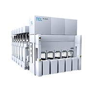
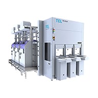
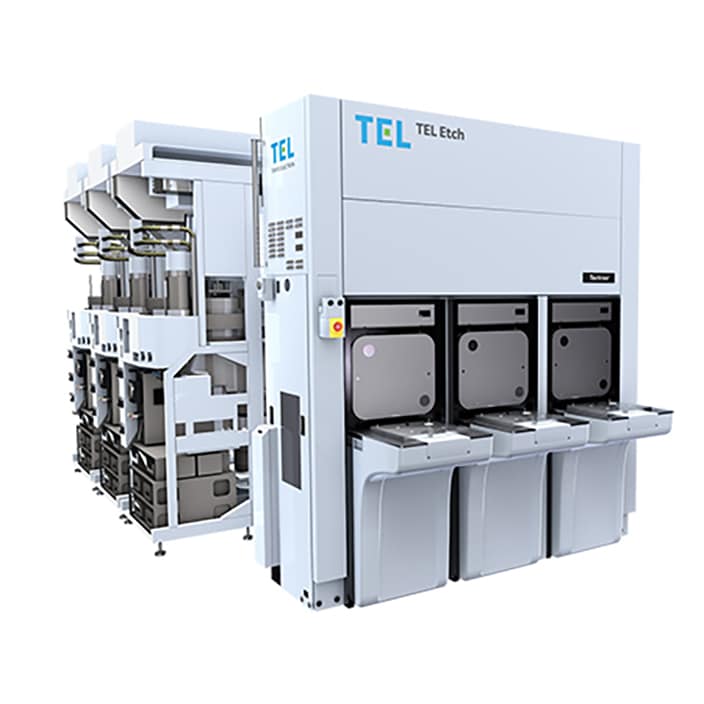
Tactras™ is a series of pioneering plasma etch systems featuring a space-saving rectangular cluster design. Since its launch in 2006, Tactras™ has evolved to achieve the world's highest level of wafer transfer speed and footprint and continues to be relied on by many customers.
Tactras™ is a highly reliable 300mm plasma etch system that enhances etch process productivity. Scaling at advanced technology nodes makes the etch process more and more crucial. Tactras™ provides customized solutions for high aspect ratio holes, trench etch, mask and dielectric etch, and BEOL dielectric etch. The common base product design allows, Tactras™ to be built for specific applications. Yield improvement is required even as the device structure is becoming more complex. As device structures have become more complex with a greater number of process steps involved, the improvement of yield is more crucial than ever. The etch chambers that can be installed on Tactras™ employ optimal design technologies to achieve excellent within-wafer uniformity, low wafer-to-wafer variation, and high selectivity in shaping the etch profile. This ensures that all etch requirements of respective applications are satisfied while high etch rates are attained to deliver high productivity. Up to 6 chambers can be installed on Tactras™, each capable of handling different etch applications as required. Tactras™ offers operational advantages enabled by TEL’s cumulative knowhow on production technology, including a robust design to minimize machine-to-machine and chamber-to-chamber variation, particle reduction technology, unit-assembly inspection, and labor-saving automation, all of which contribute to customers’ productivity.
Product comparison
 |
 |
 |
|
| Wafer size (mm) |
300 | 300 | 300 |
| Availability | New | New | New |
| Number of chambers | 1-6 | 1-12 | 1-6 |
| Application | Dielectric, Conductor, Reactive Ion Etch |
Dielectric, Conductor, Reactive Ion Etch |
Dielectric, Chemical Dry Etch |
| Substrates | Si | Si | Si |
| Safety | S2, CE | S2, CE | S2, CE |
Tactras, Episode, Certas and Certas LEAGA are registered trademarks or trademarks of Tokyo Electron Group in Japan and/or other countries.

