3D Integration Synapse™/Ulucus™ Series
Support mass production of 3D integration with reliable technology
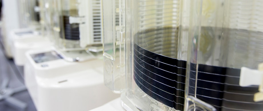
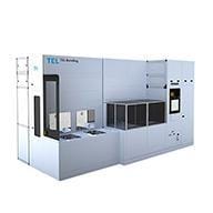
TEL’s Synapse™ series became an industry standard Bonding/DeBonding tool for 300mm wafers by combining leading-edge technologies such as ultra-thin wafer transfer, chemical coating, and plasma processing and cleaning, developed over the last 50 years. Synapse™ series is semiconductor production equipment to realize the temporary Bonding/DeBonding process in TSV (Through Silicon Via) as well as the permanent bonding process.
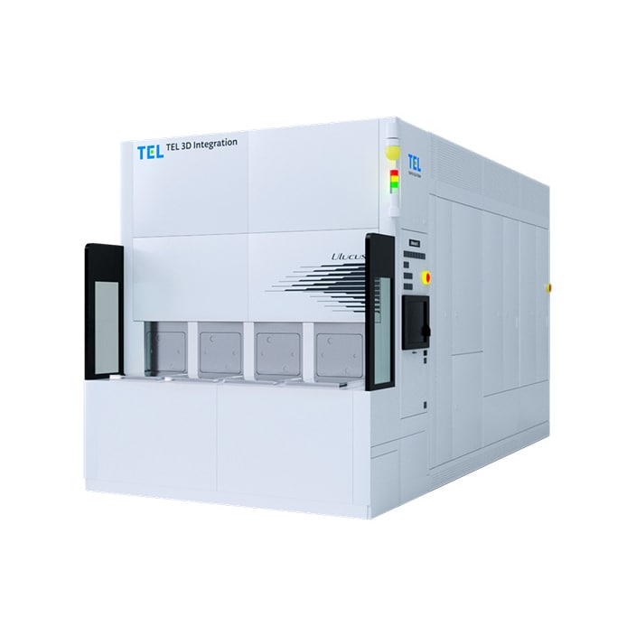
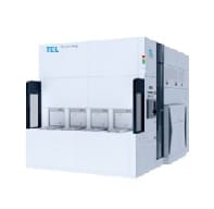
Ulucus™ L and Ulucus™ LX are semiconductor production tools integrating TEL’s Coater/Developer platform technology, with a high market share and a proven track record in mass production. The equipment contains several advanced technologies, including wafer cleaning. As further semiconductor scaling and performance enhancements are crucial to devices such as CMOS image sensors, next-generation memories, and advanced logic chips, chip manufacturers are increasingly adopting 3D high-density packaging technologies using permanent wafer bonding methods. TEL anticipates a significant growth in permanent wafer bonding processes and has introduced high-volume processing systems equipped with innovative technologies to address the customers’ production needs.
The Ulucus™ G series of semiconductor production equipment integrates TEL’s market-leading and production-proven Coater/Developer platform technology with several other advanced technologies, including wafer cleaning. Advanced patterning in semiconductor manufacturing requires increasingly higher flatness in silicon wafers. The trend of global labor shortages escalates the favorability of integrated wafer fabrication equipment that can perform multiple processes continuously and automatically. TEL anticipates significant performance improvement of semiconductors and wafer fabrication and has introduced high-volume processing systems equipped with innovative technologies to address the customers’ production needs.
Synapse™ V and Synapse™ Z Plus, these systems are 300mm wafer bonder/debonder system which enable temporary bonding or debonding process efficiently. As the continuation of Moore’s law is becoming more and more challenging, 3D-IC with through-silicon via (TSV) interconnects secure a firm position in the field of advanced semiconductor, attracting attention as a means to improve semiconductor performance. Synapse™ V is a temporary wafer bonding system, which allows two wafers to be bonded together by using various adhesives. The system consists of material coating, baking, and bonding functions to realize integrated wafer bonding processes in a single tool. Uniquely developed wafer alignment unit and wafer bonding module provide the highest level of Total Thickness Variation (TTV) and bonding accuracy. Synapse™ Z Plus, equipped with wafer debonding, device and carrier wafer cleaning function, makes it possible to complete complicated wafer debonding process after TSV process with one system. The system has newly developed special function that provides stabilize transfer and safe process operation of ultra-thin wafers less than about 50um thickness.
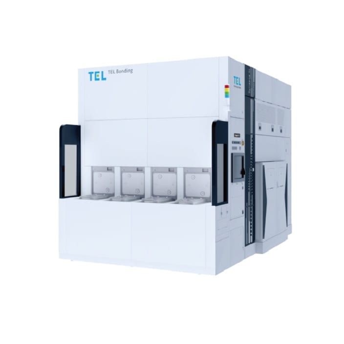
Synapse™ Si is a permanent bonding system for 300‑mm wafers that supports both fusion bonding and Cu hybrid bonding. By adopting the proven designs of the platform, cleaning modules, and plasma processing modules used in front‑end production, it delivers high-volume manufacturing reliability while achieving superior alignment accuracy and high throughput. In addition, productivity per unit area can be further increased by expanding block configurations to meet customer requirements. Permanent bonding processes are expected to expand into a wide range of applications. TEL will lead the development and mass production of these new applications.
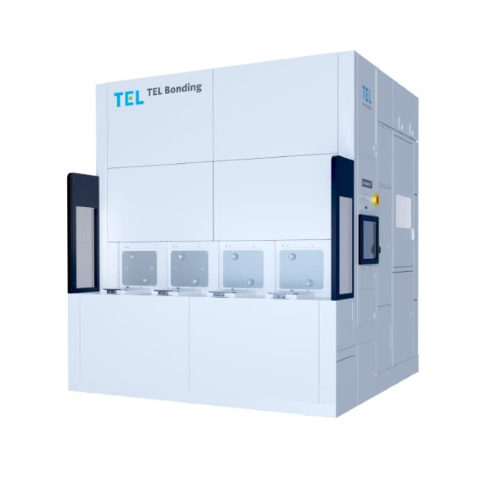
Synapse™ ZF is designed to complement Synapse™ Si, which has started to become widely adopted for mass production in many devices. It serves as a de-bonder that allows rework before the annealing process after bonding takes place. Leveraging TEL’s established debonding technology, Synapse™ ZF provides rework solution for both fusion and cu hybrid bonded wafers, helping customers improve yield, reduce manufacturing costs, and enhance quality in the permanent bonding process.
Ulucus™ L is a laser edge trimming system for 3D high-density packaging of 300mm devices. The system integrates TEL’s production-proven Coater/Developer platform technology with an advanced and highly original laser controller unit, enabling super clean technology comparable to that available in front-end processes in addition to excellent reliability and productivity. The system uses laser control technology to produce high-quality cut surfaces through precise and speedy edge trimming operations. The use of a dry laser process that does not require deionized water (DIW) ensures reduction in DIW consumption, dust emissions, and wastewater discharges. Since edge trimming is performed after the wafer bonding, fewer process steps are required before and after trimming.
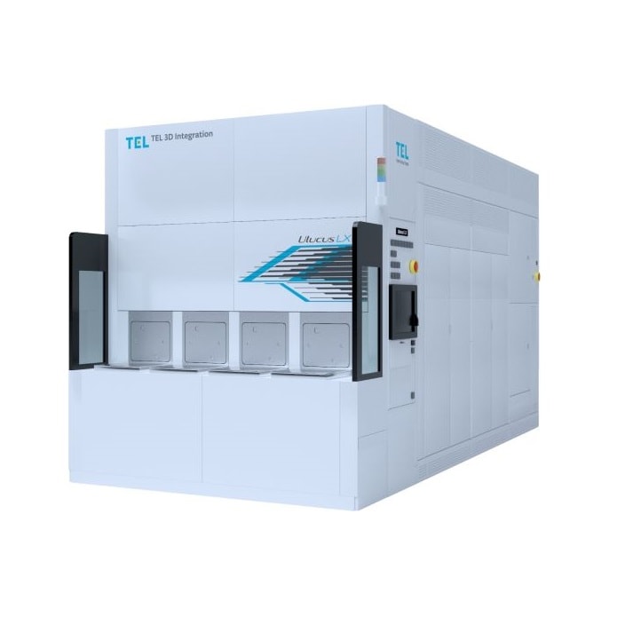
Ulucus™ LX is next-level innovation, featuring TEL’s Extreme Laser Lift Off technology and capable of performing laser beam irradiation, wafer removal, and wafer cleaning in a single unit. The system combines TEL’s advanced laser control and wafer separation expertise with the cleaning technologies cultivated in its single-wafer cleaning systems (NS and CELLESTA™ series) and integrates them on the LITHIUS Pro™ Z Coater/Developer platform.
This system will be able to replace multiple processes in permanent wafer bonding, including wafer back grinding, polishing, and chemical etching with the purpose of reusing the excess silicon wafers removed by the system. It reduces deionized water consumption by more than 90%. The system will increase the number of viable chips per wafer and reuse the excess silicon wafers.
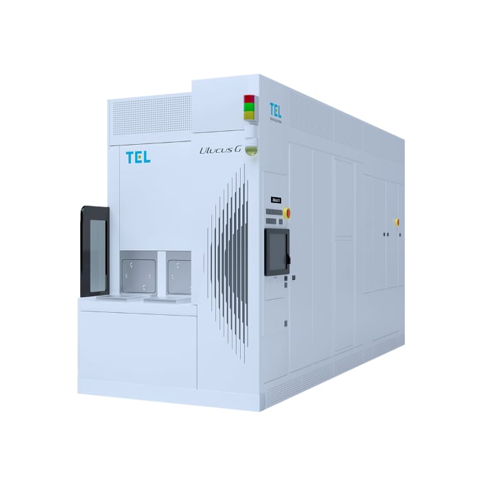
Ulucus™ G is the new wafer thinning system enabling the fabrication of higher quality silicon wafers while reducing the manpower needed for mass production. The new system integrates an originally developed grinding unit with the LITHIUS Pro™ Z platform that has been fully production-proven in coater/developer applications.
Ulucus™ G integrates the newly developed grinding unit, a scrub cleaning unit and a spin wet etch unit. All of these are single-wafer processing units which allows control over the quality of each wafer.
Inspection units can also be incorporated into the system, enabling in-system feedback and feedforward of process metrics for realizing high flatness, clean, and low damage wafer fabrication without relying on human skills.
Product comparison
 |
 |
 |
|
| Wafer size (mm) |
300 | 300 | 300 |
| Availability | New | New | New |
| Typical Applications | TSV | TSV | BSI |
| Accuracy | <5% (TTV of glue thickness) |
ー | 3σ<100nm (Alignment accuracy) |
| Additional features | Up to 3layer of glue | Mechanical-Debonding, Carrier wafer cleaning capability |
High-alignment accuracy, High-reliability |
Synapse and Ulucus are registered trademarks or trademarks of Tokyo Electron Group in Japan and/or other countries.
