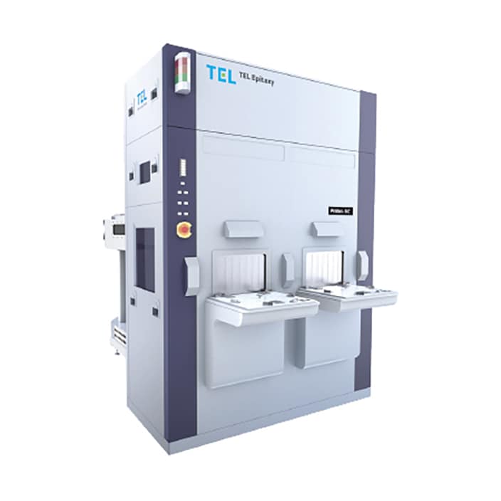
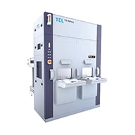
SiC Epitaxial CVD system Probus-SiC™ Series
Supporting growth of mass production of SiC power semiconductor expected as energy-saving devices by the state-of-the-art technology
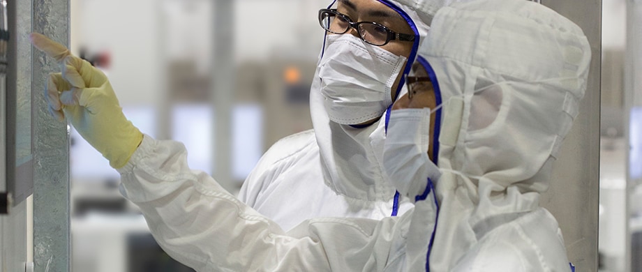
The Probus-SiC™ series is an automated SiC epitaxial film growth equipment developed by incorporating state-of-the-art technologies such as vacuum technology, transfer technology and high-temperature control technology that TEL has cultivated in the semiconductor manufacturing equipment market. We introduced the most advanced technology in the equipment at all times required by the production site listening carefully to the market needs that evolved as the SiC market grew. As a result, the equipment has capability required not only for process performance side but also for mass production side such as safety, maintenance, operability and reliability, and its performance has been highly appreciated at mass production sites all over the world.
The Probus-SiC™ is an automated SiC epitaxial film growth equipment. It is possible to install up to two semi-batched wafer process modules on the platform, and to select the equipment configuration according to the purpose from development to mass production. In addition, the tool is for 3/4/6 inches of SiC substrate and it is easy to change the wafer size simply by changing a tray called a holder, and it can easily cope with generation change of the wafer. The heating method is a hot wall type by induction heating method, which can control the high temperature up to 1,725 degrees with high precision and realizes high process performance together with the advanced side flow gas supply method. We are also working on various applications such as thin film, thick film, laminated film, Si face, C face, low off angle, trench filling etc. We strongly support customers with knowledge gained from these experiences.
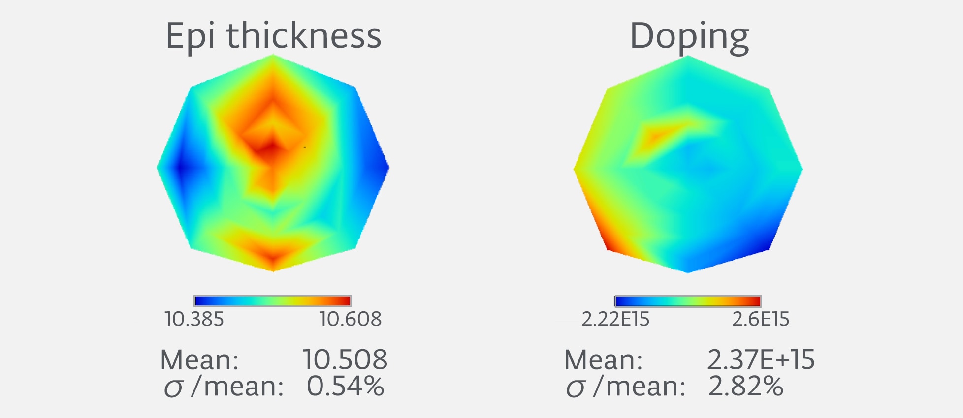
Within wafer result
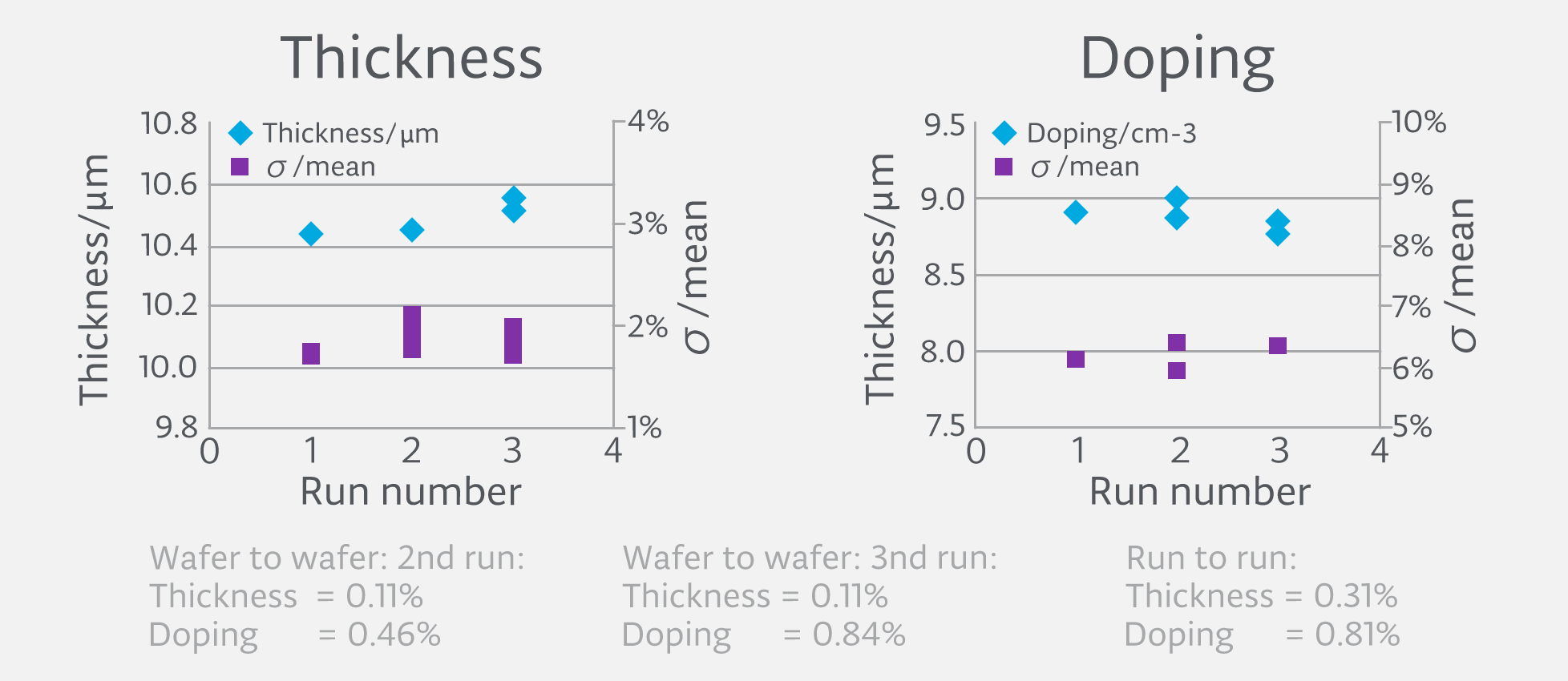
3 run/5 wafer epi repeatability
Product comparison
 |
||||
| Wafer size (mm) |
75 | 100 | 150 | 200 |
| Availability | New | |||
| Product carrier load per chamber | 8 | 7 | 3 | 1 |
| Max chambers | 2 | |||
| Throughput (process time) | <165min @10um thickness | |||
| Process temps (℃) |
1500-1725 | |||
| Chamber heating | Induction( hot wall) 1500 – 1725℃ | |||
| Safety | S2, S8, CE | |||
| Applications | Si-face, C-face, N type, P type | |||
| Additional features | Mixed wafer size vis platter | |||
Probus-SiC is a registered trademark or trademark of Tokyo Electron Group in Japan and/or other countries.
