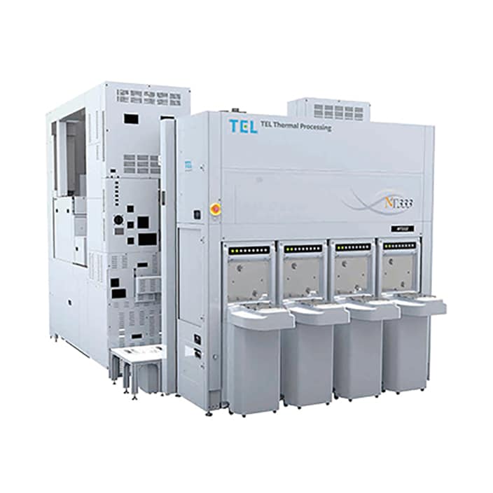
Deposition NT333™ Series
The next step for ever expanding ALD processing.
NT333™ is TEL’s first semi-batch chamber for ALD (Atomic Layer Deposition). It offers thin film thickness control at the atomic level while providing exceptional film quality and high productivity due to employment of the spatial ALD method versus more conventional time divided ALD technology. Multiple substrates can be simultaneously processed within each chamber. The chamber itself is partitioned into complementary sections enabling simultaneous exposure to and adsorption of precursors and other reactants in a continuous mode by substrate rotation. One ALD cycle is performed by one rotation of the wafer stage. No longer is ALD processing limited to ultra-thin films. High productivity ALD is now attainable by high stage rotation speeds along with an optimized gas delivery system made possible by well isolated reaction zones.
NT333™ has large wafer capacity as compared to single or dual wafer processing techniques. With the added capability of pre or post treatment steps included in each ALD cycle, NT333™ is capable of forming films of the highest quality while operating at low temperatures and providing tunable film stresses for a variety of applications. Additionally, NT333™ has unique plasma shield which mitigates plasma damage resulting in high quality films while maintain high stage rotation speeds.
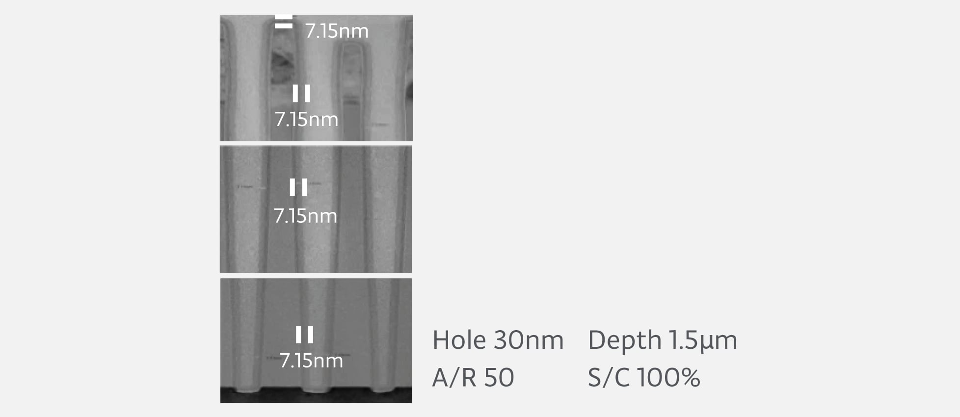
Thermal ALD SiO2 @760℃
![Etch amount [nm] @DHF](/product/pv8va20000001c6b-img/pv8va20000001ddw.png)
Etch amount [nm] @DHF
Product comparison
 |
|
| Wafer size (mm) |
300 |
| Availability | New |
| Wafer per Chamber/System | 6/12wafer |
| Process Chamber | 2Chamber |
| Reactor | Thermal/Plasma |
| Features | High step coverage, High quality film, High throughput, Stress controllability, Low plasma damage |
| Process | SiO2, SiN, High-k |
| Substrates | Si, SOI |
NT333 is a registered trademark or trademark of Tokyo Electron Group in Japan and/or other countries.
