Deposition EXIM™/ LEXIA™-EX
A flexible tool for next generation semiconductor devices
EXIM™ and LEXIA™-EX expands TEL’s product portfolio with an innovative 300mm PVD system that delivers excellent performance for forming complex multi-stack thin films. Process modules can be flexibly configured or added to accommodate various applications at different stages from R&D to high volume production. EXIM™ makes a significant contribution to the industry especially in the area of depositing multilayer films for Spin Transfer Torque Random Access Memory (STT-MRAM), a very promising next-generation non-volatile memory.In the future, with the excellent uniformity of film thickness, film quality, and film composition, and high availability as a mass production equipment, we will expand the application to advanced logic DRAM, 3D NAND etc.

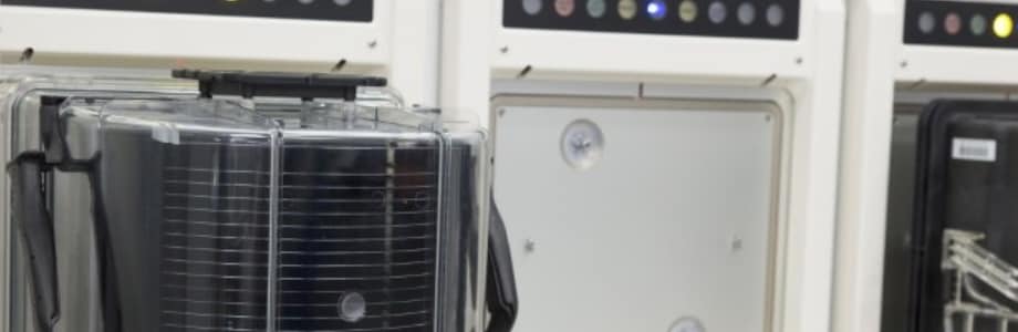
The EXIM™ is a unique flexible and extendible PVD system that provides excellent productivity for the formation of multi-layered stacks such as perpendicular Magnetic Tunnel Junctions (MTJs). Designed distinctly from typical PVD systems, the EXIM™ comprises of process and transfer modules that can be freely configured to meet challenging customer needs, from development to manufacturing. With newly developed deposition methods, the system provides improved tool up-time, low particle generation on the wafer surface, and excellent within-wafer uniformity and stability. Moreover, the EXIM™ delivers precise interface and composition control by the adoption of multiple cathodes as sputter sources. Perpendicular MTJs, key to the manufacturing of energy-saving STT-MRAM devices, may be made of more than 25 layers. The EXIM™ provides both high productivity and excellent film stack performance even for the complex processes required by such structures. With the exceptional flexibility and extendibility of the EXIM™ system, we expect the scope of process applications to expand continuously in the near future.
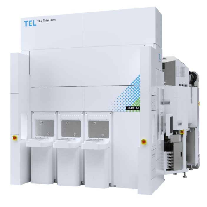
LEXIA™-EX is a sputter deposition for a wide range of applications, including advanced logic, DRAM, and 3D NAND devices.With its predecessor’s unique features such as an ultra-high vacuum chamber design to deliver superior film thickness, quality, composition, and system scalability, the footprint is about 40% smaller and CO2 emissions are 14% lower. By optimizing the transfer function, maximum throughput is 100 wph, 20% higher.In addition to the conventional four-cathod chamber (mPVD), we have developed a dPVD chamber equipped with two extra-large cathodes. This makes it possible to provide even higher deposition rates for single-layer thick film applications such as next-generation hard masks for DRAM capacitors and functional films for cutting-edge logic.
Product comparison
 |
 |
|
| Wafer size (mm) |
300 | 300 |
| Availability | Certified used | New |
| Process | Magnetic tunneling junction | Magnetic tunneling junction Metal Metal Oxide/Nitride |
| Sputtering Source | Multi cathode PVD | Multi cathode PVD Dual cathode PVD |
| Substrates | Si | Si |
| Additional features | Flexibility, Extendibility | Small footprint High throughput Flexibility, Extendibility |
EXIM and LEXIA are registered trademarks or trademarks of Tokyo Electron Group in Japan and/or other countries.
