FPD Plasma Etch/Ash
Satisfying Customer’s Needs with Overwhelming Productivity
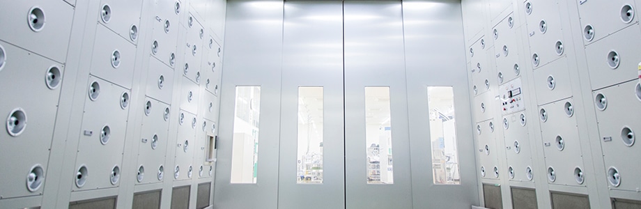
FPD Plasma Etch/Ash systems generate plasma in its vacuum chamber to etch thin-film and make electric circuits on large-area glass substrates. Our systems contribute to manufacturing liquid crystal displays (LCDs) or organic light-emitting diode displays (OLEDs) on Gen6/Gen8/Gen10.5 substrate. Since display devices get higher resolution and higher performance, FPD manufacturing increases complexity. In this background, FPD customers select TEL FPD Plasma Etch/Ash systems, which meet their requirements.
Today, to manufacture high-resolution and high-performance displays, the TFT process must become more complex, and higher productivity is required for plasma etch systems.
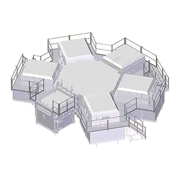
Betelex™ supports up to 5 process chambers and realize significantly higher productivity with smaller footprint and facility cost.
Betelex™ can also combine multi-process steps in separated chambers and contribute a sophisticated, up-to-date manufacturing process.
Betelex™1800 PICP™ can be applied to etch processes on LTPS (Low-Temperature Poly-Silicon) devices; metal layer (Al, Mo) etch, an insulator layer (SiOx, SiNx) etch, polysilicon layer etch or PR ash.
Features
Multi-chamber system: Maximum 5 chambers
Chamber mode: PICP™ mode
Substrate size:<Standard>
1,500mm x 1,850mm
Impressio™ is a multi-chamber Plasma Etch/Ash system supporting Gen 6 - 10.5 substrates for various applications, small/medium displays for smartphones, and large displays for TVs.
Impressio™ series can be applied to etch processes on LTPS (Low-Temperature Poly-Silicon) devices, oxide semiconductor devices, and amorphous silicon devices; metal layer (Al, Mo) etch, an insulator layer (SiOx, SiNx) etch, silicon layer etch or PR ash.
Features
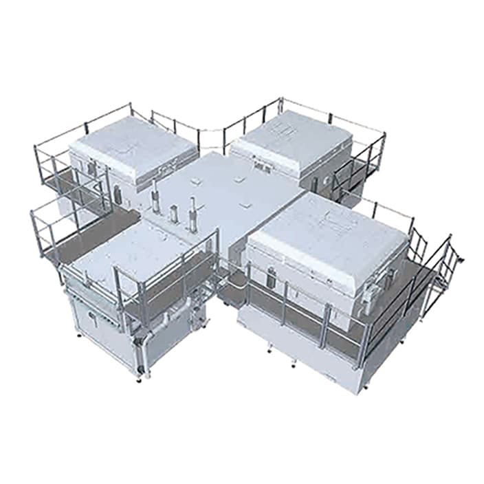
Multi-chamber system: Maximum 3 chambers
Chamber mode: PICP™ mode/PICP™ Pro mode/ECCP mode
Substrate size:<Standard>
1,500mm x 1,850mm (PICP™)
2,200mm x 2,500mm (PICP™)
2,940mm x 3,370mm (ECCP、PICP™)
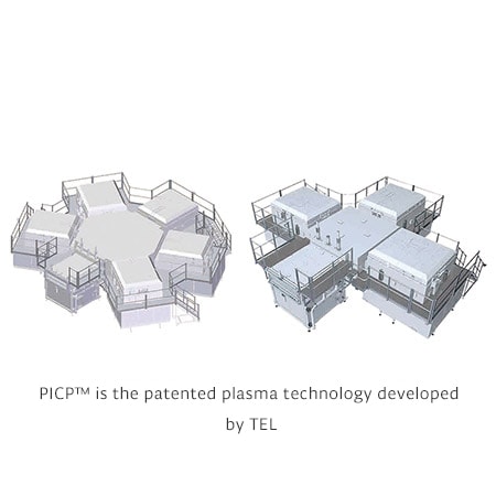
As flat panel displays for smartphones and other devices require higher resolutions, ultra-low power consumption, various innovative interfaces, or other new technologies, manufacturing FPD requires a more refined process, higher productivity, and better yield for Plasma Etch/Ash system. Responding to these needs, TEL developed PICP™, which is the plasma source with Innovative Technology and Concept for large FPD Plasma Etch/Ash system. PICP™ can produce extremely uniform high-density plasma on the substrate and significantly improves process uniformity. At the same time, it lowers power consumption by up to 20% or more (compared with previous TEL models), reducing the risk of electrostatic damage to devices and preventing process excursions in mass production.
PICP™ can be applied to etch processes on LTPS (Low-Temperature Poly-Silicon) devices and metal-oxide devices; metal layer (Al, Mo) etch, an insulator layer (SiOx, SiNx) etch, polysilicon layer etch or PR ash.
Product comparison
| Gen10.5 | Gen8.5 | Gen6 | |
|---|---|---|---|
| Market | TV | TV,Tablet,Monitor | Mobile, AR/VR, Automotive |
| Technology | LCD, OLED, a-Si,Metal Oxide | LCD, OLED, a-Si,Metal Oxide | LCD, Flexible OLED, LTPS, Metal Oxide |
| Substrate size (mm) |
2940x3370 | 2200x2500 | 1500x1850 |
| Platform | Impressio™ | Impressio™ | Betelex™ Impressio™ |
| Chamber Mode | ECCP | PICP™ | PICP™ |
| Application | Silicon layer etching, Insulating layer etching, Metal layer etching, Ashing |
Silicon layer etching, Insulating layer etching, Metal layer etching, Ashing |
Silicon layer etching, Insulating layer etching, Metal layer etching, Ashing |
Impressio,PICP and Betelex are registered trademarks or trademarks of Tokyo Electron Group in Japan and/or other countries.
