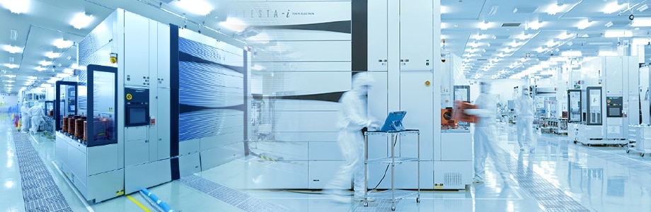
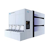
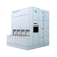
Cleaning CELLESTA™ Series
A state-of-the-art single wafer cleaning system for collapse free drying, higher productivity, and higher reliability
Surface preparation system CELLESTA™ series for 300mm single wafer clean applied cutting-edge research findings and accumulated experiences in the field. The system provides excellent performance and extendability for advanced clean and dry process with high throughput and smaller footprint. With industry-recognized high reliability and productivity, as a leading-edge cleaning system, CELLESTA™ is continually evolving to meet technology requirements and customer's needs for advanced clean with new value.
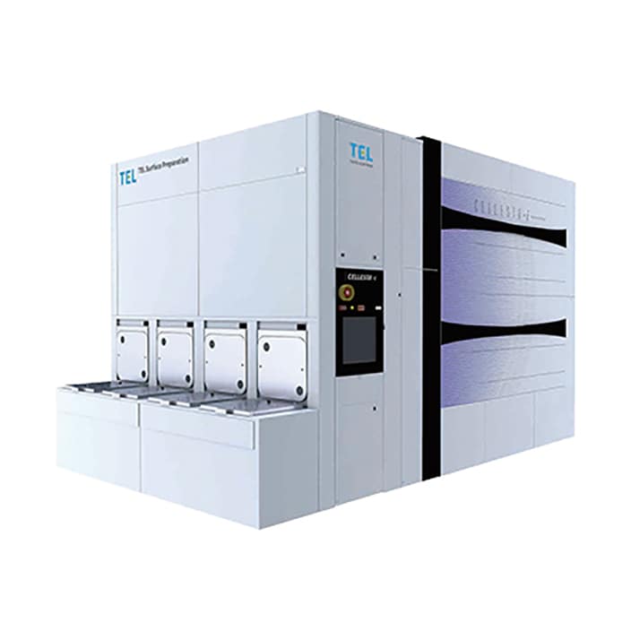
The CELLESTA™ -i MD is a TEL's most advanced 300mm single wafer clean system for 10nm technology node and beyond. The system has state-of-the-art cleaning capability which enables damage less clean of the well-patterned wafer surface and damage free particle removal. Pattern collapse free drying technology is also realized by implements of both chamber atmosphere control and performance improvement of IPA dispenser. The system has achieved higher productivity and lower running cost with the use of newly developed chemical recycle concept. The CELLESTA™- i MD offers scalability and will strongly support the establishment of the most challenging wafer surface clean process technologies using various chemicals for Cu and other metal exposed layer of next generation devices.
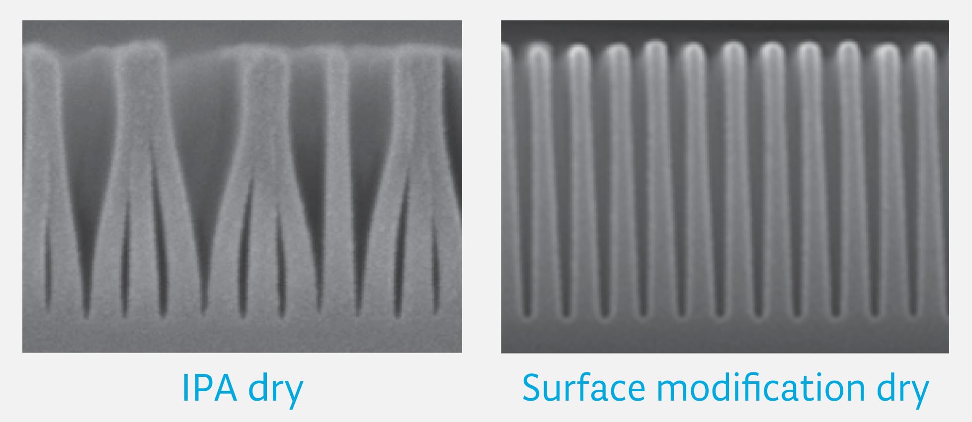
N+1 Pattern collaspe free technology

CELLESTA™ -i for 300mm wafer surface clean processing system provides enhanced productivity and significantly decreased footprint. The system incorporates up to twenty units of cleaning chambers and has much smaller footprint. Furthermore, it is equipped with integrated chemical recycle technology contributing less CoO, physical cleaning function for the particle removal on wafers; all of these functions contribute to achieve higher productivity. Additionally, this platform has excellent system extendibility, which is able to equip advanced bevel clean unit dedicated to wafer periphery and backside clean unit with less chemical consumption.
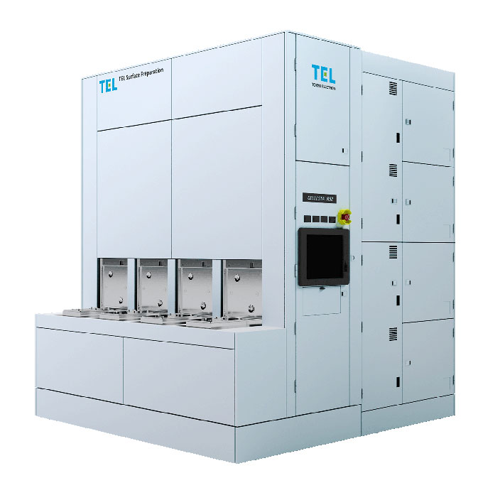
CELLESTA™ MS2 incorporates a physical cleaning function featuring dual-fluid spray technology and brushes. Its capability to process both wafer sides simultaneously significantly boosts the system’s productivity per unit area, making it over 1.5 times more productive than TEL’s previous systems when both wafer sides need to be cleaned. The system also helps to reduce the levels of utility usage while processing, because the system eliminates the use of deionized water and gases conventionally required to protect the non-washing side of the wafer. Also, TEL’s proprietary wafer retention technology enables previously challenging task of cleaning the outermost wafer edge and bevel, delivering high levels of particle control required in the manufacture of advanced semiconductors. TEL will continue to satisfy customers’ needs for advanced semiconductor manufacturing processes by offering physical cleaning technologies that further improve productivity and yield.
Product comparison
 |
 |
 |
|
| Wafer size (mm) |
300 | 300 | 300 |
| Availability | New | New | New |
| Throughput (wph) |
650 | 650 | 800 |
| Process | Pre/Post clean, Wet etch | Pre/Post clean, Wet etch | Physical force Clean |
| Substrates | Si | Si | Si |
| Dry method | New IPA dry /SMD | Hot IPA dry | Spin Dry |
CELLESTA is a registered trademarks or trademarks of Tokyo Electron Group in Japan and/or other countries.
