Solutions that Create Value for Customers
Development of Global Operations
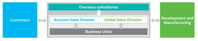
We established the Account Sales Division and the Global Sales Division and strive to swiftly offer the technology, services and solutions our customers need to become the sole strategic partner for our customers. In the Account Sales Division, we receive and leverage next-generation
technology needs shared by major semiconductor manufacturers such as those in memory, logic, and foundry businesses driving current momentum in the AI device market, to develop cutting-edge technologies. The Global Sales Division responds to the needs of domestic and overseas customers that handle products for the rapidly-growing Chinese market and the industrial IoT market.
These divisions work in close coordination with business units, development and manufacturing divisions, service divisions, and overseas subsidiaries to conduct comprehensive sales activities. By engaging in communication with our customers—from their management to on-site engineers—we continue to further strengthen our responsiveness and expand global operations as ONE TEL.
Proposing Customer Solutions Leveraging a Wide Range of Product Lineup
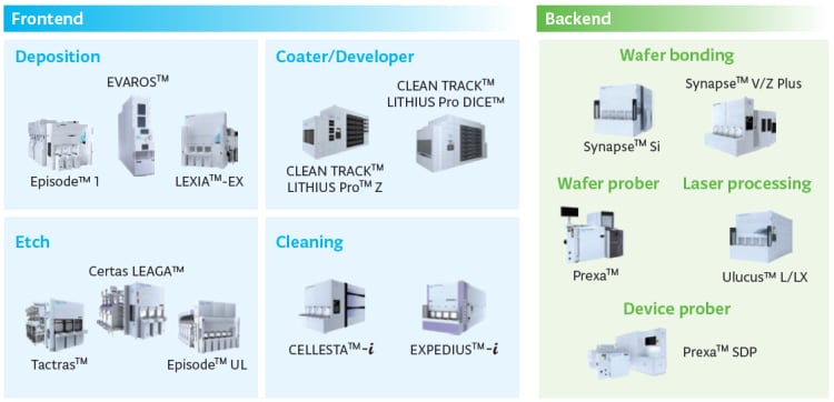
We are expanding the wide range of our product lineup, including equipment for the four key processes of deposition, coater/developer, etch and cleaning in the frontend process, as well as equipment for testing and bonding/debonding processes in the backend process. By leveraging this product lineup in our proposal activities, we will solve customers’ issues and contribute to the manufacturing of highly competitive semiconductors.
In the frontend process, we are undertaking the development of equipment with innovative and extreme processing performance, centered on (1) deposition systems that accommodate new materials and structure while utilizing batch, semi-batch and single-wafer capabilities, enabling precise control of film thickness and film quality, (2) coater/developers for EUV lithography including leading-edge High NA, (3) etch systems that enable precision patterning of fine features and the fabrication of deep holes and trenches with high selectivity, and (4) cleaning systems that remove particles and residues—which are causes of yield loss—without causing the collapse of fine patterns.
In the backend process, we also possess wafer probers used in wafer testing and bonding/debonding systems that realize 3D packaging. In the future, there will be a demand for further improvements in the performance of semiconductors as well as scaling technology using cutting-edge nodes to improve the performance in generative AI services and expand the application range. To achieve this higher performance, the adoption of advanced packaging technology (Chiplet) that combines singulated dies is accelerating. We provide KGD* test equipment, which is essential for Chiplet, and we are actively providing solutions for bonding processes of diced devices as well.
Looking ahead, as device scaling continues to advance, including through the adoption of Chiplet technology, we will provide solutions to customers’ challenges by leveraging our broad portfolio of frontend and backend products, together with our process integration capabilities that span across manufacturing processes.
KGD: Known Good Die/Device. A bare die or device that have been tested and proven defect-free.
Expansion into the Diversified Semiconductor Market
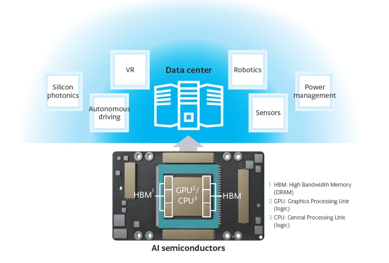
In recent years, the semiconductor market has been rapidly expanding and evolving, driven by advanced logic, memory, and advanced packaging for AI data centers, along with related technologies, such as silicon photonics and power management, as well as autonomous driving, VR, various sensors, and future robotics applications. Specialization by application as well as collaboration are advancing, and value is increasing along with changes in the entire ecosystem. Under these circumstances, we provide equipment with proprietary technologies for enabling advanced functions while also providing an optimal product lineup for new applications and a wider range of functions, drawing on our large installed base, extensive experience, and use of the latest technologies. We also propose a variety of solutions including improving the productivity and extending the service life of equipment in our installed base.
Initiatives for Improvement of Customer Satisfaction
Since our founding, we have been working to build solid relationships of mutual trust with customers by enhancing customer satisfaction, which we value highly. We co-create future technology roadmaps with the semiconductor manufacturers that are our customers to promote the concurrent evaluation of technologies for the next four generations and beyond and accelerate Shift Left development, while also striving to optimize cost. This enables us to provide optimal solutions that contribute to customer value creation and to offer highly competitive products that help improve customers’ productivity by improving the yield rate of devices and maximizing equipment utilization rate. Furthermore, at customer sites around the world, we are continuously implementing customer-oriented initiatives such as assigning our company engineers to ramp the equipment up to its maximum performance quickly, proposing effective solutions to identified technical issues and providing feedback on next-generation equipment.
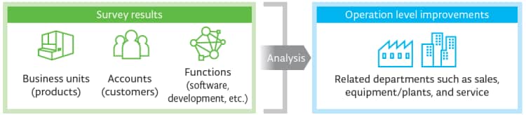
In addition to these activities, we conduct our own Customer Satisfaction Survey* every year. In the fiscal year 2026 survey, we received responses from approximately 1,800 respondents (response rate: 84.2%). We analyzed the results and used them in our PDCA cycle to make improvements at the operation level.
Our activities were highly evaluated and we received best awards consecutively from many of our customers in fiscal year 2026. We will continue to provide the Best Products with innovative technology and Best Technical Service with high added value and strive to further improve customer satisfaction.