Tackling Technological Innovation
Research and Development for Next-Generation Computing
Demand for semiconductors is increasing on a global scale and production is expected to grow even further in the future. Under such conditions, an unchecked increase in power consumption due to the growing use of semiconductors may lead to an energy supply risk in the market. In modern-day computing, focus for edge devices is placed on lower power consumption, but for the server-side the focus is more on performance rather than power consumption. This is in response to the market needs. Therefore in the future, we may need to rethink the balance of Power usage, Performance, Area of silicon, Cost and Environmental impact (PPACE) of our devices in order to address this energy issue. At Tokyo Electron, we recognize these and other issues and are working to resolve them through our semiconductor production equipment business.
One solution to the power efficiency problem is to place memory devices closer to logic devices (computational circuits). By shortening the electrical pathway, one can reduce the electrical resistance and thereby reduce power consumption during information transfer between the devices. Optimization of device architecture using this technique is effective, and development in this area has been gaining momentum in recent years.
Additionally, for logic devices, SoCs*1 that take advantage of the computing characteristics of CPUs, GPUs*2 and NPUs*3 and distribute computational tasks to the most efficient circuits are increasingly popular. This SoC architecture can be built by a monolithic process that does not use bonding technology, but can also be built using 3D system integration techniques which leverage bonding technology. Also called “heterogeneous integration*4”, 3D system integration technology combines and packages a variety of different materials such as silicon and non-silicon elements, CPUs and DRAMs*5, analog and other electronic components.
In AI technology, development of analog neural devices*6 and nonvolatile resistive random access memories*7 which mimic the energy-efficient human brain function is well underway. Our film deposition technology contributes to this development.
By combining and applying these technologies, we will be able to further reduce power consumption and improve computing efficiencies in a variety of devices.
Realizing next-generation computing requires the development of AI chipsets with an even higher processing speed and greater energy efficiency. By taking maximum advantage of a wide range of technologies and techniques from semiconductor production, we are working to create high-value-added equipment that can help meet one of the next-generation computing needs of bringing computer performance closer to that of the human brain. We are expanding the technological areas in which we can contribute by developing new materials and boosting the performance of chipsets through 3D system integration equipment offerings, which in turn optimize the power efficiency of semiconductors by realizing next-generation computing requirements.
We are also working on the development and application of quantum computing technology for the next generation and beyond.
SoC: System on a Chip, a design technique in which many or all of the functions required for system operation are mounted on a single semiconductor chip, or a chip built using this technique.
GPU: Graphics Processing Unit, a dedicated electronic circuit designed to manipulate and modify memory to speed up the generation of images used for displays.
NPU: Neural network Processing Unit, a processor dedicated to AI that incorporates a neural network that is modeled after the human cranial nervous system.
Heterogeneous Integration: Packaging that unites different kinds of chips
DRAM: Dynamic Random Access Memory. A type of semiconductor memory used in the main storage unit (or other electronic devices) of a computer as a large-capacity working memory
Analog neural devices: Electronic devices capable of continuously changing resistance
Nonvolatile Resistive random access memory: Random access memory that uses nonvolatile resistive memory elements
Process Development with AI Using Machine Learning
We have been quick to introduce a generative AI system that is available across the Company, as AI has been more and more put to practical use in society. In addition, we are developing generative AI specialized in software for semiconductor production equipment to accelerate product development.
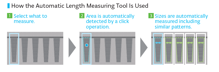
In the development for semiconductor manufacturing process, we use images taken by Scanning Electron Microscope (SEM) and measure the sizes of various microscopic structures such as linewidth and hole diameter to check process results on wafers to determine whether required results are obtained.
For this task, we have developed and used a tool applying machine learning so far, but preparation for measuring new shapes has taken long hours. In fiscal year 2024, we developed a new image length measuring tool that can measure any shape quickly and easily. With this new tool, preparation for measurement is no longer required and engineers involved in the process development can measure shapes on wafers by a simple operation, increasing productivity in process development.