Research and Development
Research and Development for the Future
With the evolution of ICT, electronics are more and more indispensable to people’s lives. In addition, there is an increasing need to realize both the development of a data-driven society and preservation of the global environment, with the growing demand for semiconductors, which is the base of ICT and increasing global awareness of the environment. The performance required of semiconductors is also becoming more diversified.
In order to contribute to the development of a dream-inspiring society, Tokyo Electron is engaged in R&D with an eye on the future to capture changes in society, including innovations in manufacturing technology and the pursuit of ultra-efficient productivity.
Market Heading toward Diversification
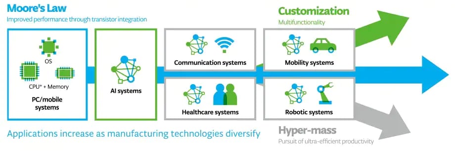
CPU: Central Processing Unit. A semiconductor chip that serves as the brain of a computer.
Strengthening Research and Development Capabilities
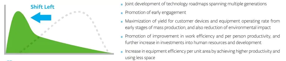
We are focusing on the promotion of Shift Left that strengthens R&D to bring high-value-added next-generation products into the market in a timely manner. Shift Left is an initiative that enables the understanding of customers’ potential needs at an early stage and the prompt delivery of mass-produced prototypes by collecting resources in the early stages of product development processes. Close collaboration with customers in leading-edge technological development contributes to ensuring the competitive advantage of products and rapidly bringing technological innovation to the market.
Furthermore, through the promotion of DX that looks to the future, we promote development to create innovative products while aiming for more efficient R&D through data analysis using AI and the automation of processes. Simultaneously, we are also expanding programs for the recruitment and fostering of DX human resources.
In addition, R&D sites, business divisions and the Corporate Innovation Division unite to advance R&D, and we are strengthening global open innovation and collaboration between industry and academia to develop advanced technology and to create new values in the future.
Through such initiatives, we respond to changes in the global business environment and the demands of society and strive to ensure high quality products and product security that meet the expectations of our customers. We aim for continued growth as a company while contributing to balancing the digitalization and preservation of the global environment while supporting the evolution of the semiconductor industry
R&D sites
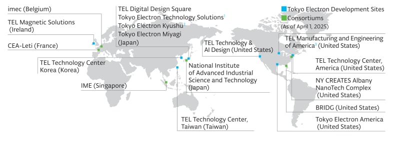
Fujii Head Office, Hosaka Office, Tohoku Office
Koshi Head Office, Ozu Office, Fukuoka Office
Chaska Head Office, Chelmsford Office
Further Strengthening of Development Structure
We are actively investing with a focus on further growth as we endeavor to further strengthen our development structure.
To this end, we have completed construction of Miyagi Technology Innovation Center and a new development building at Tokyo Electron Technology Solutions Hosaka Office. We also opened and operated new development buildings at Tokyo Electron Miyagi and Tokyo Electron Kyushu from 2025.
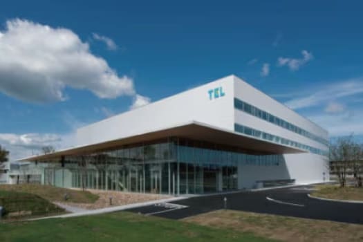
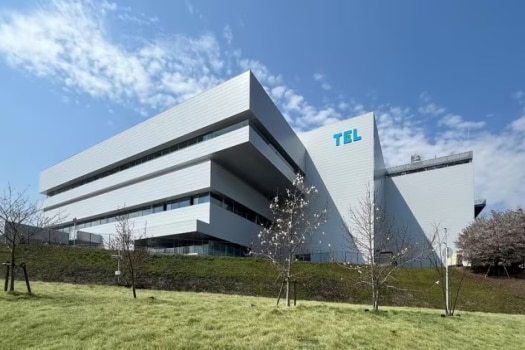
Miyagi Technology Innovation Center
(Completed in September 2021)
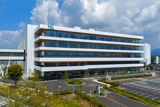
Tokyo Electron Technology Solutions
Hosaka Office New Development Building
(Completed in July 2023)
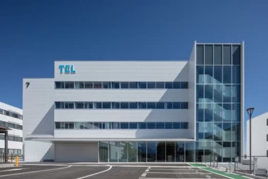
Tokyo Electron Miyagi
New Development Building
(Completion in April 2025)
Tokyo Electron Kyushu
New Development Building
(Completion in October 2025)
Shift Left
We are focused on using the Shift Left approach, investing resources such as technology, personnel and expense into the early processes of product development. Through this approach, we are endeavoring to develop various technologies and conducting research for multiple future generations to realize the technology roadmaps we have created with customers.
With product development through the Shift Left approach, we understand customer needs at an earlier stage, reflect the information obtained from feedback into our technological development and propose superior products. This contributes to maximizing yield for customer devices and capacity utilization of their mass production line equipment. We are also promoting on-site collaboration for early delivery of evaluation equipment to customers' fabs and development and research laboratories, and are working to accelerate the process in which technological development is reflected in mass production equipment as well as to optimize development efficiency.
Intellectual Property Management
We are promoting intellectual property (IP) management under the fundamental tenet of contributing to an increase of corporate profits by supporting our business activities through IP protection and its utilization.
To achieve sustainable growth in the semiconductor industry where the growth is driven by technological innovation, we are globally expanding our R&D activity including industry-academia collaborations. Our IP department collaborates with R&D departments and business departments at each of our R&D and production sites, and with the marketing department at headquarters. The aim is to provide appropriate protection for innovations created based on development seeds and market needs, and to build an IP portfolio that is compatible with our R&D strategy and its shift-left focus.
In 2023, the number of inventions created in Japan was 1,186 and 303 overseas. We have maintained the global patent application rate approximately 75% for 5 consecutive years, and the allowance rate* of the filed patents has reached 81% in Japan and 80% in the United States. Furthermore, various inventions have been created through collaboration with domestic and overseas business partners, consortium and academia, and we have jointly filed patent applications on 61 inventions in the past three years.
Consequently, the number of active issued patents as of March 31, 2024 is 23,249, which is the largest number in the semiconductor production equipment industry, and we are building our competitive edge in the intellectual property field on a global level.
Our patent portfolio has also been rated highly for aspects such as impact on other companies and improved technological value over recent years. As in 2024, we have again been selected in the Clarivate Top 100 Global Innovators 2025 and the LexisNexis Innovation Momentum 2025: The Global Top 100.
We consider IP to be an important asset for improving medium- to long-term corporate value. We will therefore continue striving to improve the competitiveness of our products through differentiation of our technologies by building a competitive IP portfolio in terms of both quantity and quality.
Figures calculated in 2023
