Tokyo Electron Launches Ulucus™ LX, an Extreme Laser Lift Off System for 300mm Wafer-Bonded Devices
Tokyo Electron (TEL; Head Office: Minato-ku, Tokyo; President: Toshiki Kawai) today announced the launch of Ulucus™ LX, an Extreme Laser Lift Off system for 300mm wafer-bonded devices.
With the advent of the AI era, the need to improve the performance and energy efficiency of semiconductor devices is more pressing than ever. As a result, 3D integration using permanent wafer bonding technology has become essential to the continued evolution of semiconductor devices. As a critical technology for high degrees of integration along with device scaling, permanent wafer bonding is increasingly in demand for the production of diverse semiconductor devices. These devices often require multiple bonding processes, making the technology hurdle even more challenging. Under these circumstances, the polishing and grinding steps to remove the unnecessary portion of silicon wafers requires a large amount of DI water during processing, and leads to reduced yield and a limitation on the number of available chips. Instead, an innovative technology is needed that contributes both to sustainability and productivity improvement.
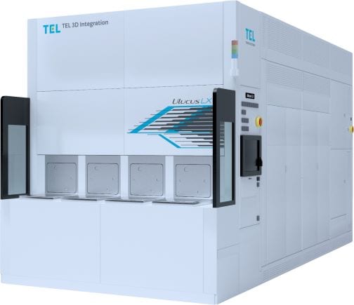
Ulucus™ LX is an innovative system designed to meet this need, featuring TEL’s Extreme Laser Lift Off technology and capable of performing laser beam irradiation, wafer removal, and wafer cleaning in a single unit. The system integrates TEL’s advanced laser control and wafer separation expertise, with the cleaning technologies cultivated in its single-wafer cleaning systems (NS and CELLESTA™ series) and the LITHIUS Pro™ Z Coater/Developer platform that has a large installed base.
Customers using this system will be able to replace multiple processes in permanent wafer bonding, including wafer backgrinding, polishing, and chemical etching, while reducing deionized water consumption by more than 90%.* By eliminating the need for conventional edge trimming, the system also increases the number of viable chips per wafer. In addition, TEL is developing the technology to reuse the excess silicon wafers removed by this system.
“In addition to scaling, the accelerating adoption of 3D high-density packaging is further evolution of semiconductor performance,“ said Yohei Sato, General Manager of ATS BU at TEL. “Wafer bonding is one of the most critical steps in 3D packaging. Of particular interest is the post-bonding wafer thinning process, where there are high expectations for a technological breakthrough. The newly released Ulucus™ LX system with Extreme Laser Lift Off technology is an innovative solution that helps improve productivity and reduce environmental impact. TEL will continue to develop and introduce advanced technologies and products that meet the needs of our customers.”
* An estimate by TEL based on a comparison with conventional wafer backgrinding and edge trimming processes.
Ulucus, LITHIUS Pro, and CELLESTA are registered trademarks or trademarks of Tokyo Electron Group in Japan and/or other countries.
For product purchase queries, please contact
For use of product photo, please contact
Corporate Communication Dept., Tokyo Electron
- tel
- +81-3-5561-7004
- telpr@tel.com
