Tokyo Electron to Collaborate with imec-ASML Joint High NA EUV Research Laboratory
Tokyo Electron (TEL; Head Office: Minato-ku, Tokyo; President: Toshiki Kawai) announced today the company will introduce its leading-edge Coater/Developer to the imec-ASML joint high NA EUV research laboratory (joint high NA lab) in Veldhoven, the Netherlands. The equipment will be integrated inline* with EXE:5000, ASML’s next-generation high NA EUV lithography system with a 0.55 numerical aperture (NA), scheduled to be operational in 2023. By collaborating with imec and ASML, TEL will continue to pursue technological development to meet the ongoing scaling needs of its customers.
High NA EUV lithography is expected to provide more advanced pattern scaling solutions compared to conventional EUV lithography. The Coater/Developer being introduced to the joint high NA lab will feature advanced capabilities which are not only compatible with widely used chemically amplified resists and underlayers, but are also compatible with spin-on metal-containing resists. Spin-on metal-containing resists have demonstrated high resolution and high etch resistance, and are expected to enable finer patterning. However, metal-containing resists also require sophisticated pattern size control as well as metal contamination control on the backside and bevel of the wafer. To meet these challenges, the Coater/Developer being installed at the joint high NA lab comes with leading-edge process modules capable of handling metal-containing resists.
Combined with the new process modules, a single unit of TEL Coater/Developer can process a wide variety of materials inline, including chemically amplified resists, metal-containing resists, and underlayers. This will enable flexible fab operation, while also realizing increased productivity and high availability that are among the advantages of a Coater/Developer.
Taking advantage of the breadth of its products spanning several adjacent processes, TEL is forming a partnership with resist materials suppliers to provide comprehensive patterning solutions covering etch processes as well as Coater/Developer for lithography processes.
Yoshinobu Mitano, TEL Corporate Director, Senior Vice President and General Manager of SPE Business Division, said, “TEL is honored to collaborate with imec and ASML at the joint high NA lab to further understand and solve the challenges of high EUV NA patterning. By leveraging our experience in high volume manufacturing of EUV lithography process technology, we intend to deliver high NA EUV process solutions to our customers’ fabs in a timely manner.”
Keiichi Akiyama, Vice President and CTSPS BU General Manager of TEL, commented, “As the manufacturer currently holding 100% of market share in inline Coater/Developer for EUV lithography, we look forward to working with the joint high NA lab to realize the most advanced Coater/Developer for next-generation high NA EUV lithography. In collaboration with our partners, we will introduce and validate cutting-edge approaches and technologies to address our customers’ challenges.”
Rudi Cartuyvels, Chief Operating Officer and Executive Vice President R&D of imec, stated, “For more than 25 years imec and TEL have been strategic partners in developing innovative solutions to advance semiconductor scaling. imec is looking forward to continuing this collaboration with TEL to enable the next step on the semiconductor scaling roadmap, high NA patterning.”
Steven Scheer, Vice President Advanced Patterning, Process and Materials at imec, said, “The collaboration between TEL and imec has been key in identifying and eliminating critical defects in EUV patterning with spin-on resist, contributing to the introduction of EUV in high volume manufacturing. For high NA EUV patterning, with thinner resist films and at smaller feature sizes, defect reduction will be even more important. Therefore, imec is pleased to be working with TEL and resist material suppliers in the Joint imec-ASML High NA Lab to enable an accelerated introduction of high NA EUV in the industry.”
* Inline: The state of being a part of a continuous process line. In this instance, it refers to the integration of a lithography system and a Coater/Developer, which means a smaller footprint and higher productivity for customers.
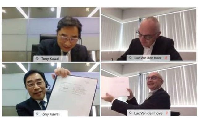
Toshiki Kawai, President & CEO of TEL (left) and Dr. Luc Van den hove, President and CEO of imec, at a remote signing ceremony of an MOU (Memorandum of Understanding) for the introduction of advanced Coater/Developer to the imec-ASML joint high NA EUV lab.
About imec
Imec is a world-leading research and innovation center in nanoelectronics and digital technologies. Imec leverages its state-of-the-art R&D infrastructure and its team of more than 4,500 employees and top researchers, for R&D in advanced semiconductor and system scaling, silicon photonics, artificial intelligence, beyond 5G communications and sensing technologies, and in application domains such as health and life sciences, mobility, industry 4.0, agrofood, smart cities, sustainable energy, education, … Imec unites world-industry leaders across the semiconductor value chain, Flanders-based and international tech, pharma, medical and ICT companies, start-ups, and academia and knowledge centers. Imec is headquartered in Leuven (Belgium), and has research sites across Belgium, in the Netherlands, Taiwan and the USA, and offices in China, India and Japan. In 2020, imec's revenue totaled 680 million euro.
Imec is a registered trademark for the activities of imec International (IMEC International, a legal entity set up under Belgian law as a “stichting van openbaar nut”), imec Belgium (IMEC vzw supported by the Flemish Government), imec the Netherlands (Stichting IMEC Nederland), imec Taiwan (IMEC Taiwan Co.), imec China (IMEC Microelectronics (Shanghai) Co. Ltd.), imec India (IMEC India Private Limited), imec San Francisco (IMEC Inc.) and imec Florida (IMEC USA Nanoelectronics Design Center Inc.).
Further information on imec can be found at www.imec-int.com
About TEL
As a leading global company of innovative semiconductor and flat panel display (FPD) production equipment, TEL engages in development, manufacturing, and sales in a wide range of product fields. All of TEL's semiconductor and FPD production equipment product lines maintain high market shares in their respective global segments. TEL provides outstanding products and services to customers through a global network in the U.S., Europe, and Asia.
Please visit www.tel.com for more information.
