Tokyo Electron Technology Solutions Completes Construction of New Development Building
Tokyo Electron (TEL; Head Office: Minato-ku, Tokyo; President: Toshiki Kawai) announced that its development and manufacturing subsidiary, Tokyo Electron Technology Solutions, has completed its new development building at the Hosaka Office in Nirasaki City, Yamanashi Prefecture. The completion ceremony was held earlier today.
As the shift toward a digital society accelerates technological innovations, the market for semiconductors is expected to grow significantly. The products developed and manufactured by Tokyo Electron Technology Solutions are also poised for sizable growth in the coming years. This growth will be an outcome of constant advancements in patterning technologies* that are crucial to making semiconductors more diverse and complex with even finer line width. The completion of the new development building will further strengthen TEL’s technology development capabilities, enabling timely delivery of products with functions that meet the needs of the market and our customers. This in turn will contribute to sustainable medium- to long-term growth of the company and to the advancement of society.
Continually adhering to the motto of Best Products and Best Technical Service, TEL will work with our customers to pursue semiconductor technology innovations that are essential to achieving both digitalization and decarbonization. As we celebrate the 60th anniversary of our founding this year, we take this milestone as a new starting point for our further challenge and evolution to contribute to the development of a dream-inspiring society.
* TEL is the only semiconductor production equipment manufacturer in the world that offers system solutions for all four sequential patterning processes that include deposition, coating/development, etch, and cleaning.
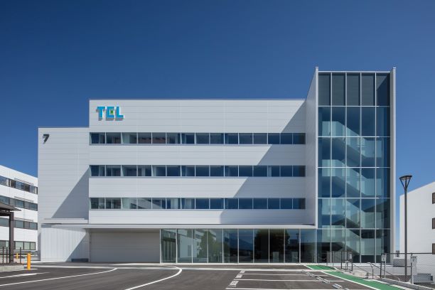
[Building Summary]
Location: 650 Mitsuzawa, Hosaka-cho, Nirasaki City, Yamanashi
Total floor area: Approx. 21,000 m²
Structure: Steel frame structure with a base isolation system
Number of floors: 4 above ground, 1 basement
Construction start: December 2021; Completion: June 2023
Purpose: Development of semiconductor production equipment (including deposition and gas chemical etch systems), development of patterning and process integration technologies
[Business Profile of Tokyo Electron Technology Solutions]
Head office: 2381-1 Kitagejo, Fujii-cho, Nirasaki City, Yamanashi
Offices: Hosaka, Tohoku, Fuchu, Nagoya Satellite
Line of business: Development and manufacture of thermal processing system, single-wafer deposition system, gas chemical etch system, test system, and FPD plasma etch/ash system
For requests to use photo, please contact
Corporate Communication Dept., Tokyo Electron
- tel
- +81-3-5561-7004
- telpr@tel.com
