Is “Measuring” the Essence of Semiconductor Manufacturing?
TEL’s Advanced Measurement Technologies
Technology
Semiconductors are ultra-precise components at the core of smartphones, PCs, and cars. In their manufacturing, even nanometer-level deviations or performance errors are unacceptable. That’s why highly accurate measurement technologies are essential.
This article highlights the importance of “measurement” in semiconductor manufacturing and guides you through the unknown world of measuring.
The Role of “Measurement” in Semiconductors
The semiconductor manufacturing process involves many complex steps. To ensure that the shapes and dimensions match the design, various kinds of “measurement” are essential.
For example, in NAND flash memory (512GB), which is used widely in storage devices like SSDs, USB drives, and SD cards, about 400 inspections and measurements are performed across roughly 1,000 process steps.
Getting the intended measurements ensures performance reliability. Measurement not only supports quality control but also helps improve processes and increase yield rates—the percentage of good products.
For these reasons, Tokyo Electron (TEL) has been steadily developing its own measurement technologies. Development environment under harsh conditions such as vacuum, plasma, temperatures above 1000°C, or very low temperatures between -100°C and -150°C (or even lower), requires accurate temperature measurement devices. If no suitable technology exists, TEL creates its own measuring tools. This approach shows how closely TEL engages with measurement technology.
Measurement Technologies Used by TEL
Next, we will introduce some of the measurement techniques TEL uses on-site.
Optical Film Thickness Measurement Before and After Processes
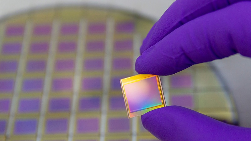
Semiconductor manufacturing involves building up multiple thin films to form tiny circuits. Film thickness measurement checks whether the film thickness matches the design during layering and processing steps.
The thickness of semiconductor films directly affects how electronic parts operate and conduct electricity. If it is too thick or too thin, it can cause defects or reduce performance. Because of this, film thickness measurement is a basic and frequently used technique throughout many process steps.
How is it measured?
In semiconductor production, optical film thickness measurement is commonly used. This method shines light on the film to be measured, then calculates the thickness from the pattern of colors and intensities in the reflected light (interference waveform).
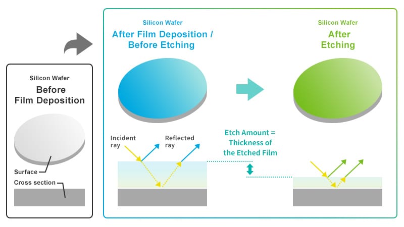
For example, soap bubbles reflect surrounding light and sparkle with rainbow colors. The thickness of the bubble’s film varies in different areas, causing differences in the interference patterns, which makes the colors appear different depending on the spot. Similarly, the thin films in semiconductor manufacturing show different colors and reflections depending on the location, allowing us to calculate their thickness from these patterns.
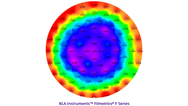
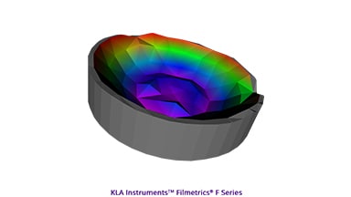
Visualizing film thickness variations (non-uniformity) using color distribution and 3D maps
(Images provided by KLA)
There are various types of films, and if the material allows light to pass through, optical film thickness measurement can be used. For films that do not transmit light or cause strong scattering, optical methods are difficult. In such cases, thickness is measured by combining other technologies such as lasers or contact-type step gauges.
Introduction to a Measurement Case
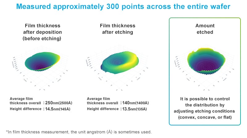
Here is an actual example of etching a wafer with a film. Using a film thickness measurement tool, we measured 300 points across the entire wafer. The results are shown in the 3D map below. A silicon nitride film of 250 nm was formed on the wafer using a thin film deposition system. There is a height difference of 14.5 nm between the thicker and thinner parts of the film (left image).
After plasma etching reduced the film to the required thickness, the overall film thickness decreased to 140 nm. The difference between the thick and thin areas became 13.5 nm. The film thickness distribution, originally concave, also changed (middle image). This change is due to different etching speeds at the center and edges of the wafer. By adjusting the etching conditions, we can control this distribution (right image). In this way, we fine-tune the thickness and variation between the center and outer edges.
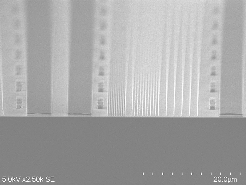
Measuring Invisible Surface Bumps and Hole Depths with SEM (Scanning Electron Microscope)
SEM is a technology used to measure ultra-fine surface bumps on wafers. It can observe nanometer-scale structures that are invisible to optical microscopes. SEM measures “surface conditions” and “three-dimensional dimensions” that are too small to see, such as circuit pattern widths, defects, hole depths, and cross-section shapes.
How is it measured?
First, the wafer is carefully broken using a special tool to create a sample piece about 3 to 4 mm in size. The sample is placed in a holder, and an electron beam is directed at it with the SEM to visualize surface bumps. Areas that reflect more signals from the electron beam appear white, while areas with fewer signals appear black.

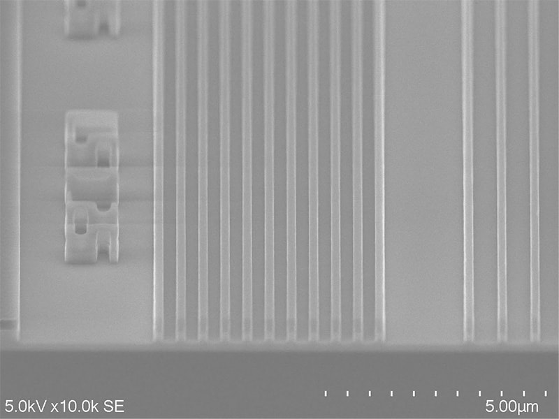
1. Creating (cleaving) a sample suitable for measurement from a wafer is a very difficult and requires skilled craftsmanship.
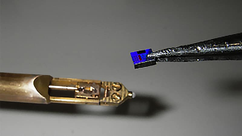
2. Set a sample piece of about 3 mm in size into the holder.
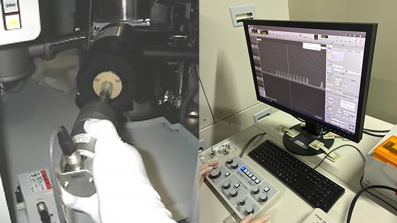
3. Attach the holder to the SEM and start the measurement.
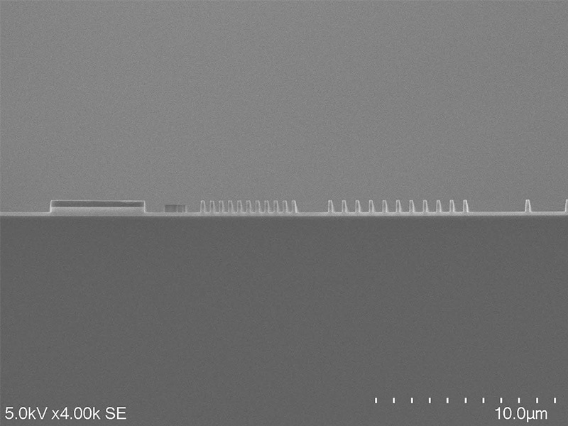
4. Search for the observation area at low magnification (left photo shows the corner of the sample piece).
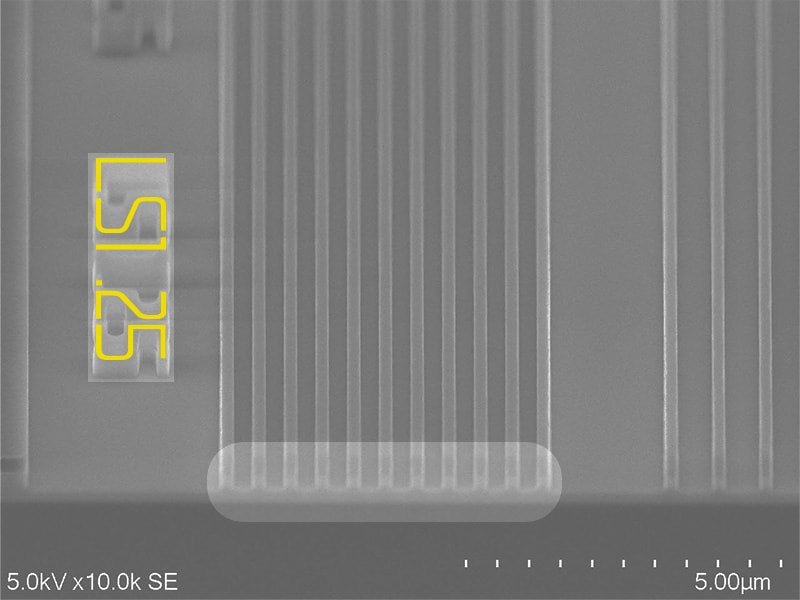
5. Observation point (“LS 1.25” Line and space interval is 1.25 times)
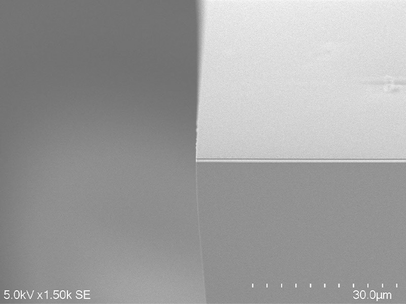
6. To observe the cross-section, position the sample so that its angle is horizontal.
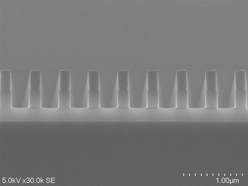
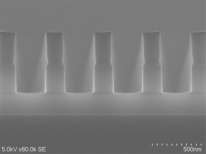
7. Gradually increase the magnification from 30,000× to 60,000× and “capture” the images.
Source of Photo 1-7: TEL
“Measuring” is Choosing the Right Technology and Quantifying Shapes and Functions
This time, we introduced film thickness measurement and SEM, but there are many measurement technologies used in the semiconductor manufacturing process. Typical examples include photolithography dimension measurement, electrical property measurement, impurity/element analysis, crystallinity measurement, and topography measurement.
As this variety of technologies shows, choosing the right technology is very important in semiconductor measurement. For example, using an optical measuring instrument on a film that does not transmit light, or trying to measure nanometer-scale features with a ruler that only works at the micrometer scale, is meaningless. You must fully understand the measurement principles and applications to select the appropriate technology.
Measurement is an essential process in semiconductor manufacturing. Measurement is not just a process of checking the condition, but an important step that supports the entire manufacturing process. Only accurate measurements can produce high-performance, highly reliable semiconductor products to release onto the market.
Share
