TEL’s R&D at the Forefront of the Advanced Packaging Era
Technology
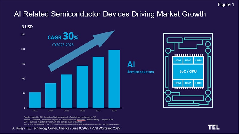
In recent years, rapid advancements in artificial intelligence (AI) and high-performance computing (HPC) have driven significant growth in the semiconductor market that supports these technologies. AI semiconductors sales are forecasted to grow at a compound annual growth rate (CAGR) of 30% through 2028, reflecting a remarkable expansion in demand for AI chips and highlighting the importance of R&D efforts in driving improvements in computation speed, capacity, and efficiency
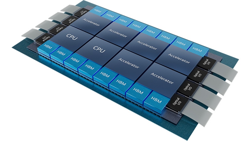
AI semiconductors are manufactured using “3D Integration” (3DI) technology, which packages multiple chips and functions into a single unit, enabling further performance improvements in semiconductors. This technology is currently attracting great attention as a key enabler for enhanced semiconductor capabilities.
Leveraging its extensive equipment portfolio, Tokyo Electron (TEL) is accelerating research and development of 3DI equipment by utilizing digital twin technology. This article introduces TEL’s initiatives toward further technological innovation in 3DI, based on a presentation by TEL engineer Angélique Raley at the prestigious international conference Symposium on VLSI Technology & Circuits 2025 (VLSI Symposium).
Biography
-

Angélique Raley
Angélique Raley is currently Sr. Director of Technology in Integration and 3DI at TEL Technology Center, America. She oversees R&D efforts to integrate TEL’s equipment portfolio solutions in advanced logic, packaging, and photonics. She earned her M.S. in Materials Science and Engineering from Polytech’ Grenoble, France, and started her career at Samsung in integration before joining TEL in 2010. Angélique is an active member of the semiconductor research community and sits on the organizing committees of several international conferences. Throughout her career she has contributed several conference papers, invited talks and has over 50 granted patents to the steadfast advancement of key semiconductor technologies.
Why is 3D Integration Technology Key to Semiconductor Evolution?
3D integration (3DI) technology combines multiple semiconductor devices or different materials into a three-dimensional structure within a single package, enhancing performance and functionality.
Until now, semiconductors have improved performance mainly through “scaling”: writing circuits more finely within smaller 2D areas. 3DI technology has recently emerged as a new approach to semiconductor development that complements 2D scaling.
The growing demands for high-speed, low-latency data processing from applications such as AI, HPC, autonomous driving, and 5G/6G have created a need for semiconductor technology. The high-density, high-functionality semiconductor packages enabled by 3DI are indispensable for further improving semiconductor performance and features, drawing significant attention.
At the VLSI Symposium 2025, Angélique Raley served as the organizer of a session focused on sharing challenges in the evolution of 3DI technologies and gave an overview of the potential for post bond overlay control through digital twin enablement.
Session member Tagami Masayoshi from KIOXIA highlighted the importance of 3DI technology in accelerating evolution of 3D NAND memory scaling, while Stanford University PhD student Dennis Rich presented an ultra-dense 3D Heterogeneous integration concept N3XT. Dr. Liron Gantz from NVIDIA spoke at the session and explained the growing importance of interconnecting bandwidth to avoid bottlenecks. He discussed NVIDIA co-packaged optics (CPO) technology – packaging technology in chiplet design that connects multiple semiconductors at high density to improve performance and efficiency — and the need to explore advanced 2.5D and 3D integration architectures to enable further scaling and efficiency.

Expanding Use of 3DI Technology in Front-End Processes
Semiconductor manufacturing is divided into “front-end” and “back-end” processes. The front-end process forms semiconductor devices on a substrate called a wafer. The back-end process involves dicing the wafer into individual chips and assembling them into finished products.
Each process requires different technologies; however, recently, there has been technical convergence where bonding techniques traditionally used in back-end processes are applied in front-end processes, and vice versa. Both processes require manufacturing equipment with ultra-high cleanliness and precision.
This technical convergence arises from increasing needs for advanced, high-density semiconductor packages to achieve higher performance and functionality. Specifically, wafer bonding technology*—previously used in CMOS image sensor manufacturing—is now applied in front-end processes for 3D NAND and logic devices. Additionally, bonding technology development is accelerating for DRAM. It is anticipated that bonding technology will be introduced across all next-generation major semiconductor devices, making it an essential technology. Depending on the specific semiconductor device roadmap, different bonding techniques will be , required to drive accelerated development.
*Wafer bonding technology: A technology for bonding multiple wafers (semiconductor substrates) together. It is used to join different layers in 3D integration.
TEL’s Strength: Products Integrating Both Front-End and Back-End Technologies
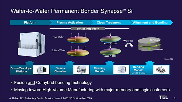
Developing bonding equipment, requires integrating many technologies. TEL possesses a broad product lineup covering both front-end and back-end processes, with expertise in high-precision and ultra-clean technologies demanded in front-end processes, holding a high global market share in each area. Few manufacturers worldwide can offer such broad equipment portfolio under one umbrella. Leveraging this strength, TEL develops equipment that integrates technologies from both front-end and back-end processes. Optimizing bonding interfaces with plasma activation and cleans processes, controlling CMP, and ensuring proper film properties such as thermal conductivity, are all critical to the final bonding and device performance. Development of semiconductor process technologies and hardware leveraging knowledge from conventional front-end equipment such as etching, deposition, cleaning, and surface preparation is accelerating.
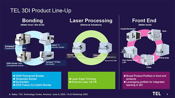
◆ TEL’s 3DI Equipment Lineup
Wafer Bonding Equipment “Synapse™ Si”
Designed to meet the stringent requirements unique to 3DI by applying front-end technologies such as plasma control*, cleaning, and high-precision alignment. This equipment consolidates bonding process technologies known as Cu hybrid or Fusion.
* Plasma control technology: A technique that manipulates gases and high-energy plasma for precise processing of semiconductor surfaces.
Temporary Bonder/Debonder “Synapse™ V and Synapse™ Z Plus”
Integrates TEL’s front-end spin coating*, cleaning/drying technologies, and proprietary position control technology to enable processing of Through-Silicon Vias (TSVs) on thin Si device layers. This technology is critical for manufacturing HBM (High Bandwidth Memory), whose demand is rapidly expanding for AI semiconductors.
*Spin coating technology: A technique that spreads liquid over the surface of a rotating wafer to create a uniform thin film coating.
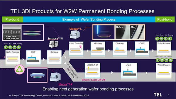
Edge Trimming System “Ulucus™ L”
Utilizes specialized laser processing to precisely trim wafer edges with high process cleanliness and reliability. Ulucus™ L is developed based on the platform of the highly mass-produced front-end lithography equipment* LITHIUS Pro™ Z.
*Lithography equipment: A system that creates patterns of semiconductor circuits on wafers.
Extreme Laser Lift-Off (XLO) System: Ulucus™ LX
A wafer de-bonding technique that uses a specialized laser to remove a silicon carrier wafer, which can then be reused again and again. This process conserves the silicon carrier wafer and reduces water usage to significantly reduce the environmental impact of wafer processing.
Accelerating Development Using Digital Twin Technology
To develop high-performance equipment, it is essential to understand and identify key factors through validated simulation models. TEL employs digital twin technology* using physics-informed machine learning (Physics AI)* modeling methods. This approach maintains necessary prediction accuracy even with limited training data, accelerating development speed. Models and optimizations must translate into actual product performance to be meaningful. Comparing different correction models through tests, conducting simplified short-loop trials for learning, and identifying hidden factors are crucial.
* Digital twin: A technology that accurately replicates the operation of real devices or equipment on a computer, used for design and optimization.
* Physics AI: An AI / Machine Learning technology that specifically integrates known physics relationships to create highly accurate predictive models even with limited data.
Challenges to Overcome in Developing 3DI Equipment Include:
- Managing Wafer Warpage Accurately bonding warped wafers requires correction technologies that are tailored to the degree and specific shape of warpage.
- Minimizing Post-Bond Distortion The bonding process is driven by a combination of mechanical and chemical phenomena that can create localized distortions in the bonded wafers. Hardware design and process condition optimization are needed to control the bonding process and thereby control the post-bond distortions.
- High-Precision Alignment and Overlay Measurement Using infrared cameras to measure wafer positional shifts, analyzing translation, rotation, scale changes, and residual errors. Evaluation and improvement of bonding accuracy are required.
To address these challenges, TEL promotes optimization in virtual environments using digital twin technology, precisely reproducing elastic deformation of upper and lower wafers, pressure at the center, air pressure and friction at bonding surfaces, and wafer release actions. This greatly contributes to reducing prototype iterations and shortening development time.
All Aimed at Contributing to Semiconductor Technological Innovation
3DI technology is an essential element for realizing advanced applications including AI. Its widespread adoption demands sophisticated technology development and close collaboration between equipment manufacturers and semiconductor makers. TEL leverages its broad equipment portfolio and proprietary integrated learning platform, dramatically improving development efficiency through physics-based digital twins, and accelerates equipment development to meet the emerging needs of the semiconductor industry. Going forward, TEL will continue to be a key player supporting the further expansion of 3DI technology in enabling the semiconductor industry of the future.
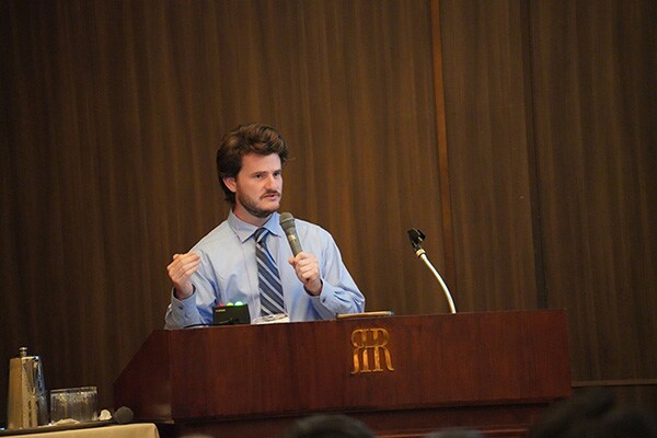
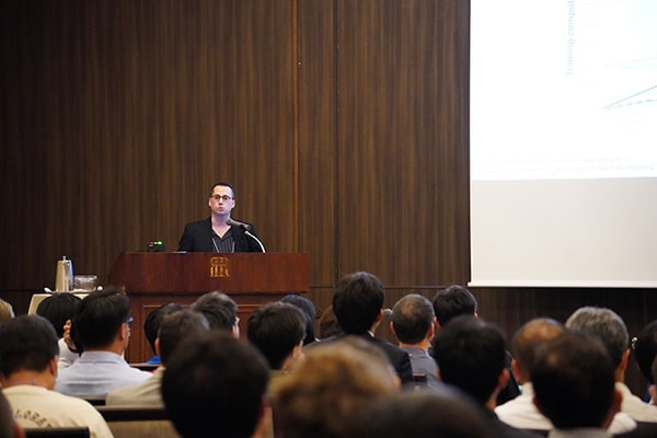
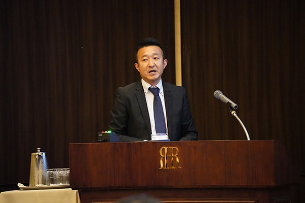
Below is a selection of photos from the session.
