Digital Twins Accelerate Innovation in Semiconductor Technology
Technology

In recent years, digital twin technology has emerged as a focal point in the semiconductor production equipment industry. Digital twins are virtual representations of real-world objects and systems. They simulate the behavior of their physical counterparts, facilitating optimization through real-time data analysis and prediction. This technology is expected to streamline production processes, enhance development efficiency, and ultimately accelerate the evolution of semiconductors.
In the following article, Hironori Moki—who leads a team of data scientists in the Equipment Intelligence & Application Development Dept. at Tokyo Electron (TEL)—explains the latest developments in digital twin technology and its applications.
Biography
-

Hironori MokiVice President, Equipment Intelligence & Application Development Dept.
Moki joined TEL in 2000 as a software engineer to develop software for controlling semiconductor production equipment. In 2011, he participated in a machine learning adoption project, developing error detection and process control systems for TEL’s equipment. In 2020, he transferred to Tokyo Electron Miyagi and joined a DX promotion project in the process development field. He has held his current position since 2024, leading the equipment intelligence and application development team.
Digital Twins and Semiconductor Production Equipment
Could you first explain what a digital twin is?
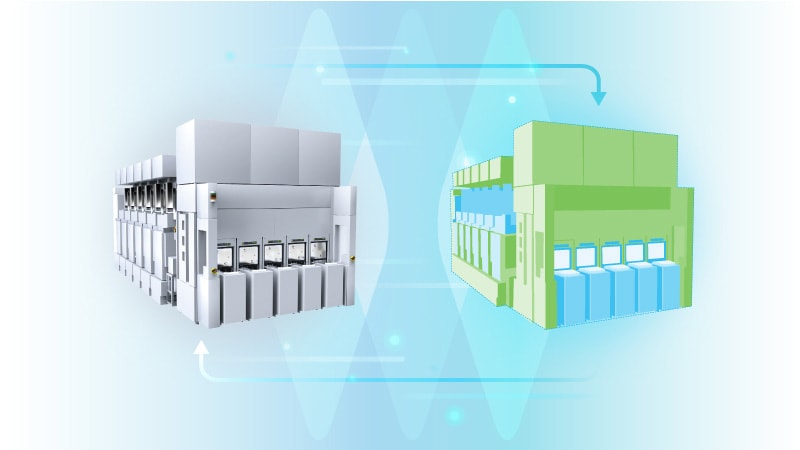
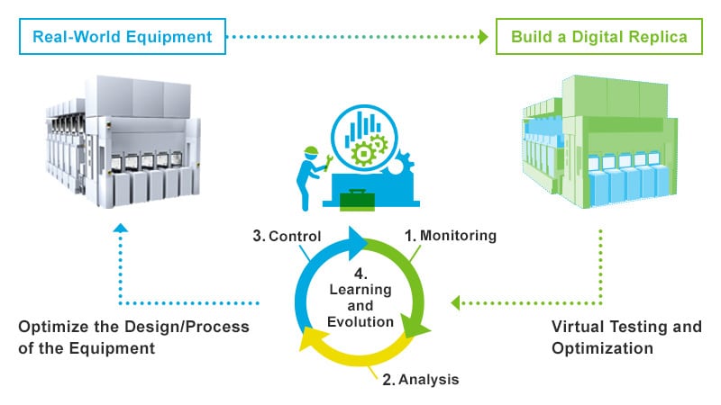
A digital twin is essentially a virtual replica. Using simulation technology, it replicates a real-world object, system, or phenomenon within a computer system. Digital twins closely mimic reality in a virtual space. This allows us to test various predictions and scenarios in a controlled environment to determine the optimal parameters. These results can then be applied to real-world design and development operations, potentially leading to improvements and solutions to problems.
Could you give us some examples of how digital twins are used in semiconductor production equipment?
Digital twin technology can create virtual replicas of semiconductor production equipment. We then use these replicas to run forecasts, conduct research, and make improvements in cyberspace before implementing changes to the actual equipment. That’s the general idea.
Digital twins of semiconductor production equipment allow us to observe, analyze, and predict the impact of real-time changes to equipment designs and process conditions.* This enables us to obtain critical hardware information, such as optimal dimensions, without building a physical prototype. We can also explore different process conditions before processing actual wafers. Since various conditions can be tested in cyberspace, optimal solutions can be reached with fewer prototypes and experiments.
*Process conditions: Process conditions refer to the technical specifications applied to semiconductor manufacturing processes ,including deposition, lithography, etch, cleaning, and testing. These conditions can significantly impact the performance and production cost of semiconductor devices.

Why are digital twins necessary for research and development (R&D)?
Advances in semiconductor device scaling and production equipment have complicated the development process and exacerbated the time- and cost-related issues. One way to address these issues is to use computer-aided engineering (CAE)* and AI, as in digital twins. Due to recent and projected advancements in computing, the industry has reached a consensus that conducting R&D without CAE and AI is no longer practical.
*Computer-aided engineering (CAE): Technology that uses computers to conduct product simulations prior to production to identify issues and improve designs.
Tell us more about the complexities involved in developing semiconductor production equipment.
Consider, for example, the task of searching for and identifying the optimal set of process conditions (i.e., recipe) from numerous variables. A few decades ago, the typical number of candidates was around 5,000 or so, but now it has grown to 106-108. Conducting a hundred million experiments to identify a single recipe is simply impractical, especially if the experiments have to be done manually.
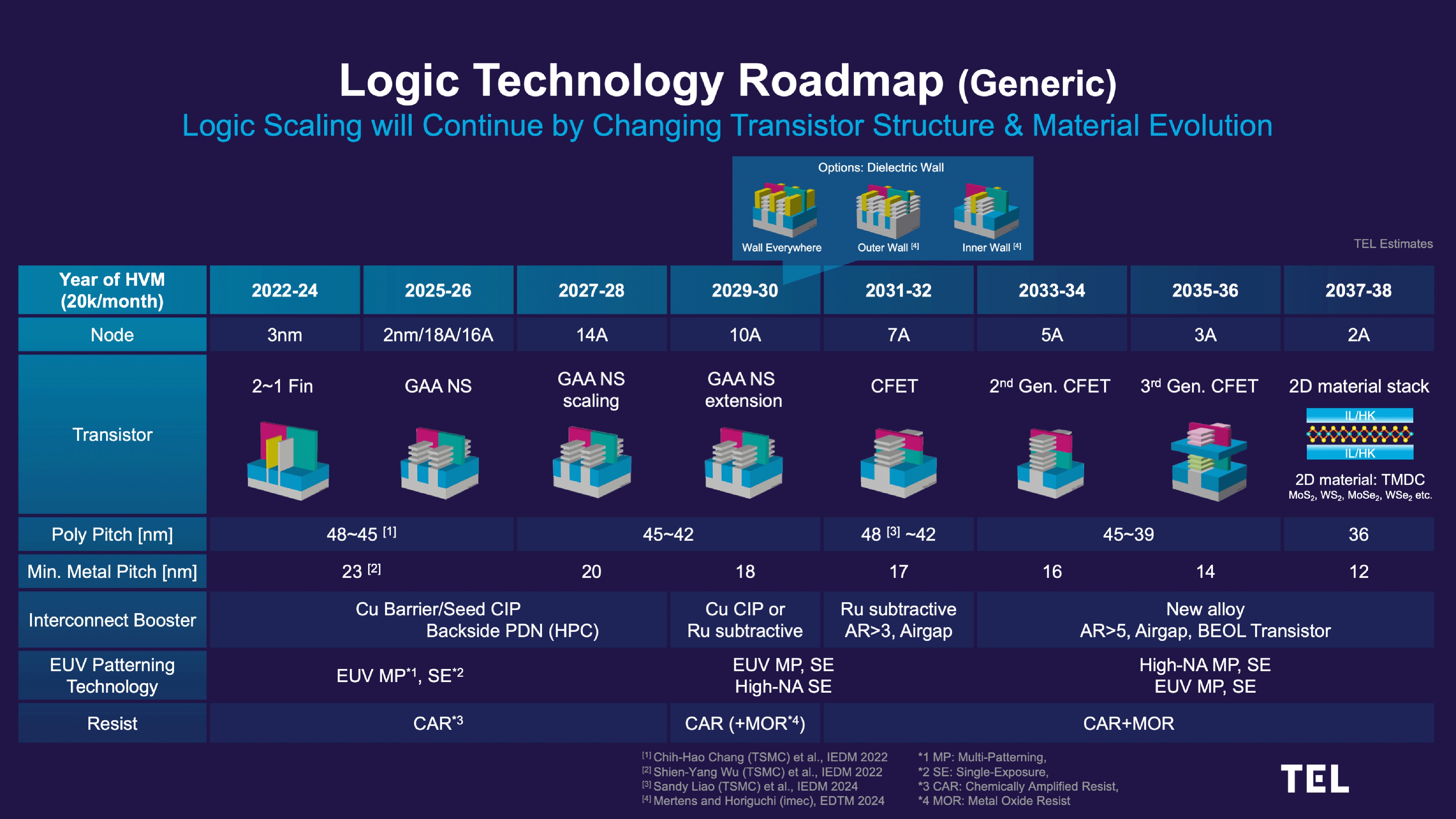
Furthermore, the development of semiconductor devices has become significantly more complex due to the introduction of three-dimensional (3D) structures. 3D chip profiles must be observed from both vertical and horizontal cross sections. This is impossible with conventional 2D simulations and measurements. As semiconductor development becomes increasingly more complex, semiconductor equipment manufacturers including TEL must proactively adopt new approaches and technologies to enable the sustainable evolution of semiconductors.

Simulation Technology and Machine Learning: Two Pillars of Digital Twins
What makes TEL’s use of digital twins special?
TEL has adopted digital twin technology for two reasons.
Firstly, using digital twins means fewer physical prototypes and experiments are needed. It leads to shorter development periods, reduced environmental impact, and lower costs. Secondly, as TEL is a leading semiconductor equipment manufacturer, we possess detailed hardware configuration data and in-depth knowledge of process mechanisms. These resources enable us to create digital twins with greater confidence and precision. Our ability to perform highly reproducible virtual experiments gives us a competitive edge, allowing us to develop products with high precision and under optimal process conditions.
How precise is the replication process?
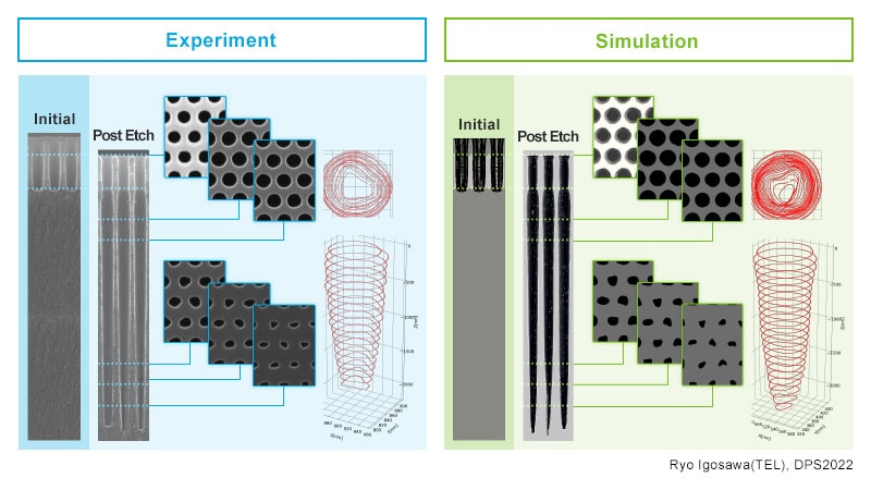
Take a look at the pictures below. The one on the left is based on real experiments, while the one on the right is a reproduction based on virtual experiments. The close resemblance between the two images is proof of the high reproducibility of our virtual experiments.

This is an example of a digital twin that was created to simulate a wafer etching process. In a physical experiment, a wafer must be sliced to observe its cross sections. In contrast, a digital twin enables us to virtually view any cross sections without cutting the wafer.
What technology enables high-precision digital twins?
Most machine learning models are typically data-driven, meaning they can make sufficiently accurate predictions within the bounds of available data. However, the accuracy of these predictions decreases significantly when the query exceeds the range of the acquired data. Furthermore, it is challenging to gather sufficient data in the fields of semiconductors and semiconductor production equipment because these fields advance rapidly, with hardware configurations and process technologies updated every few months. To overcome these challenges, TEL uses an approach known as physics AI,* a machine learning model that integrates the laws of physics to ensure accurate predictions even with relatively little data.
*Physics AI: An approach that integrates the laws and models of physics into artificial intelligence (AI) to enhance its capabilities.
All for Driving Semiconductor Technology Innovation
Lastly, please explain the benefits that digital twins bring to TEL.
As semiconductor devices advance toward further scaling with 3D structures, the demand for high-value-added solutions using CAE and AI will be greater than ever. Digital twin technology will become a necessity, not just an option. And it will play an increasingly important role, one that is fundamental to semiconductor evolution.
TEL leads the industry with over 25,000 patents and a substantial amount of real-time technical data, which is generated by a large installed base of semiconductor equipment that grows by 4,000 to 6,000 units per year (as of March 2025). TEL also possesses a vast amount of technological data spanning hardware configurations and process mechanisms. With all these data at its disposal, TEL is creating various digital twins by integrating simulation and AI technologies, with the goal of finding optimal solutions faster with less manpower to advance R&D.
The industry needs more people involved in this new approach to development. The semiconductor market has huge growth potential and is expected to nearly double its size by 2030. If you are interested in improving our society by advancing semiconductor technology, I urge you to take the plunge. A good place to start is academic conferences and industry events such as SEMICON, where you can learn about the latest technological advances and network with others to gain insight into the industry. If you become curious about semiconductors, I consider it a win.


