Episode™ 2 DMR, a Single-Wafer Deposition System Based on an Innovative Concept—the Story behind Its Development and Evolution
Technology
With the Episode™ series of single-wafer deposition systems, TEL addresses customer needs for device scaling, transitioning to 3D device structures, and diversifying film deposition materials. The products in this series are capable of handling complex deposition processes to achieve excellent productivity and environmental performance.
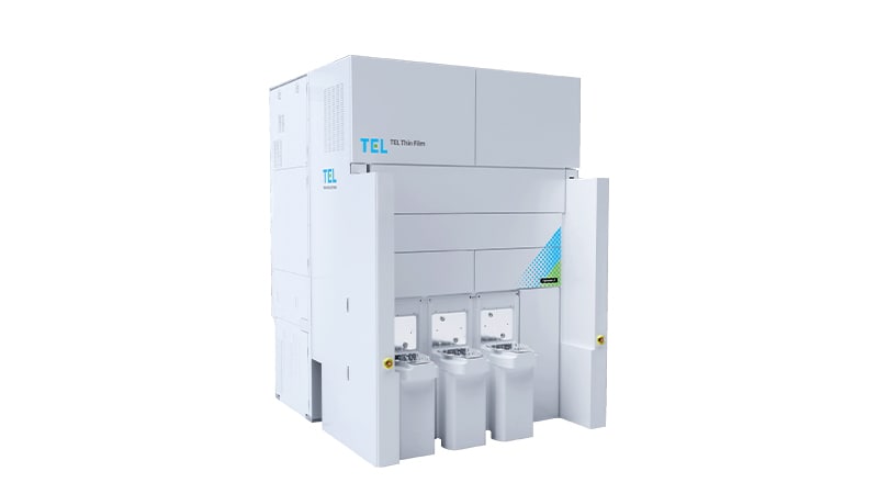
This article focuses on Episode™ 2 DMR (Duo Matched Reactor), one of the products in the series. Built with a design concept that differs from its predecessors, Episode™ 2 DMR combines a smaller tool footprint with high productivity, achieving a 25% reduction in CO2 emissions. Let us examine the development process of this system, its advanced design concept and features, and the TEL development team responsible for its creation.
TEL’s unique design concept gave life to Episode™ 2 DMR
The key to ensuring the continued evolution of semiconductors is the shrinking and 3D expansion of devices. One of the latest examples is 3D NAND flash memory, which consists of vertically stacked memory cells. While this three-dimensional design dramatically increases the data storage capacity, it also presents new manufacturing challenges, particularly in film deposition. More stacks mean more areas to coat, and ensuring uniform deposition further increases throughput time.
This has led to increased customer demand for a system that can deposit film faster and in greater quantities and with a smaller tool footprint than before. Recognizing the trend toward multiple single-wafer processing and the growth of the deposition system market, TEL has developed Episode™ 2 DMR, a highly productive system with a reduced footprint. This new system, the successor to the Triase+™ EX-II™ TiN series that has been widely used by various memory manufacturers, can process two wafers simultaneously.
Novel “multiple single-wafer deposition” system concept
To create a faster, smaller, and more energy efficient deposition system, TEL adopted the concept of dual single-wafer deposition for the Episode™ 2 DMR system, using two synchronized sets of independent reactors. During the product development phase, TEL had also explored the idea of placing two wafers in a single reactor for simultaneous deposition. However, this idea was abandoned because it could not match the fine-tuned processing realized by two independent sets of reactors. As semiconductor devices continue to shrink, it was determined that dual single-wafer deposition would better meet the technology requirements.
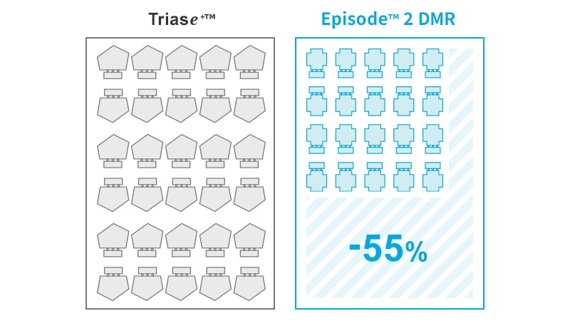
To make the system smaller, the team also rethought the layout and design of various components other than the reactor modules. For faster processing, the team developed a dual wafer transfer module and increased the maximum number of attachable chambers to 1.5 times that of the Triase+™ series. These changes significantly improved space efficiency, reducing the system footprint in a cleanroom by 55% for the same number of reactors. A smaller system requires less energy to operate the reactors, resulting in a 25% reduction in CO2 emissions.
However, the smaller system size often makes maintenance more difficult. Because semiconductor manufacturing requires regular replenishment of materials and replacement of parts, the ease of maintenance is critical. To ensure product operability, the team ran numerous simulations to determine the optimal location and accessibility of parts.
An environment conducive to rapid and thorough product development
TEL's attentiveness and passion for manufacturing underpinned the development of this system. It is often the case that product development is carried out through vertically segregated teams with specific expertise in machinery, electrical engineering, etc. Instead, TEL created the Episode™ 2 DMR project team, whose members met regularly several times a week to work closely on the development of the product.
Another highlight of this team was that many of its members came from different areas of expertise, in addition to those who had worked on the previous Triase+™ series. Behind the creation of this team, was a strong sense that we needed to think outside the box in order to develop and deliver radically new and better products at unprecedented speed. In fact, it took only a year and a half from project inception to the first shipment, which was exceptionally fast.
Speed is not the team’s only strength. As is the norm at TEL, the members are very thorough in their verification testing. The team used scale models of fab facilities and simulation software to fully validate the concept before proceeding with product development and manufacturing.
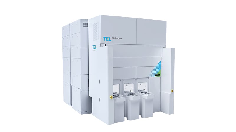
The team’s flexible and thorough approach to development ensures that the Episode™ series will continue to evolve and adapt to new device structures and materials. Currently, the team is developing Episode™ 2 QMR (Quad Matched Reactor), a deposition system capable of processing four wafers simultaneously, with full production scheduled to begin in 2026.
The Episode™ series also features an upgraded system for equipment data collection and edge information processing, which works with an analytics application to improve equipment utilization and engineer efficiency. Additionally, a number of performance-enhancing applications will be introduced in the coming years.
As Episode™ 2 QMR enhances the performance of semiconductor devices, everything that uses those devices becomes more productive, making our lives better. The availability of more advanced chipsets can result in new smartphones that are smaller, have better performance, longer battery life, and are competitively priced compared with their predecessors. This is just one example of how TEL’s technology is improving the way we live and work.
Share
