Episode™ 1 Single-Wafer Deposition System for Semiconductors: Driving the Evolution of AI Semiconductors to Transform Everyday Life
Technology
The proliferation of generative AI has led to explosive growth in the AI semiconductor market. The production of AI servers capable of processing massive amounts of data requires high-performance semiconductor devices in smaller dimensions.
As manufacturing processes also became more complex to enable device shrinking, Tokyo Electron (TEL) developed a new deposition system and launched the Episode™ series in the summer of 2024. This series is capable of performing multiple processes without interruption, offering significant productivity gains in semiconductor device manufacturing.
The following article focuses on Episode™ 1 of this series, and discusses how its features and benefits affect the speed of AI processing and the evolution of our society.
Further Evolution of AI Requires the Evolution of Semiconductor Devices
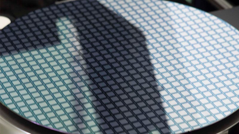
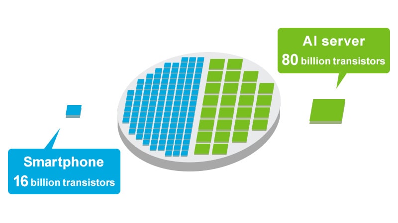
Today, we feel the growing presence of AI in everything we do. The enormous processing power of AI is supported by so-called AI servers, which contain a large number of sophisticated semiconductor devices. For example, an advanced CPU (central processing unit) embedded in a smartphone typically has about 16 billion transistors, while a GPU (graphical processing unit) that powers an AI server integrates as many as 80 billion transistors.
In other words, the processing power required by AI is far greater than that required by traditional CPUs and servers. The superior processing power and speed provided by core logic devices such as GPUs is critical to the further enhancement of AI. Advances in logic come from further shrinking of devices. The more transistors we can pack on a given area, the higher the circuit density, which makes data processing faster and more energy efficient. As AI continues to transform our society, we need to increase the pace of logic chip scaling.
The production of logic devices with smaller feature sizes requires a deposition system capable of forming a film on fine surface structures. In response to this growing need, TEL launched Episode™ 1 in July 2024.
Episode™ 1 Uses Applied Technologies to Improve Deposition Uniformity
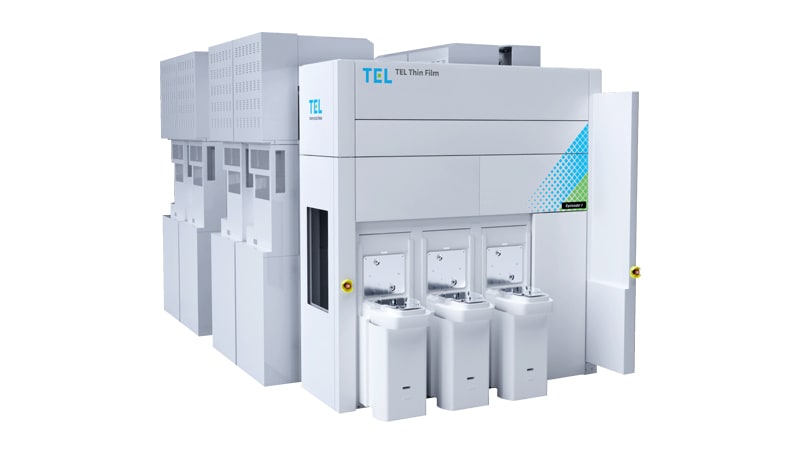
Episode™ 1 is a single-wafer metal deposition platform that can integrate up to 8 process modules, double the maximum supported by its widely used and production-proven predecessor, the Triase+™ series. As semiconductor devices continue to shrink, the system enables multiple and increasingly complex processes to run simultaneously without interruption.
The key to improving the performance of a device is to reduce the contact resistance of the interconnects. In metal deposition, any exposure of the processed wafer to oxygen and/or moisture will oxidize the deposited metal, increasing the electrical resistance. Episode™ 1 integrates multiple process modules with a vacuum wafer transport system that allows metal deposition to occur immediately after oxidized film removal, resulting in lower contact resistance compared with conventional systems.
Physical vapor deposition (PVD) has been the preferred film deposition method for many semiconductor equipment manufacturers, but when it comes to depositing materials on structures at the bottom of deep contact holes, PVD has fallen short. Meanwhile, device scaling has progressed to the point where it is necessary to deposit films uniformly on intricate structures at the bottom of deep holes.
To overcome this challenge, Episode™ 1 uses chemical vapor deposition (CVD) technology. The system fills contact holes with a titanium-containing gas, allowing chemical reactions to take place and deposit uniform films on the inner walls and surfaces of the bottom structures. TEL has over 20 years of experience in titanium CVD to produce memory chips. This expertise has proven to be applicable to the production of logic chips with 3D structures.
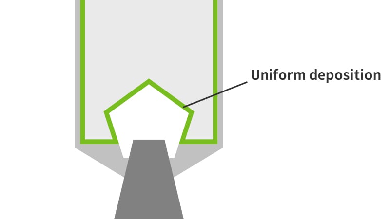
The use of CVD technology has made it possible to deposit low-resistance films uniformly even on complex structures at the bottom of deep contact holes. The processes are carried out without interruption in high-vacuum modules, resulting in better device performance.
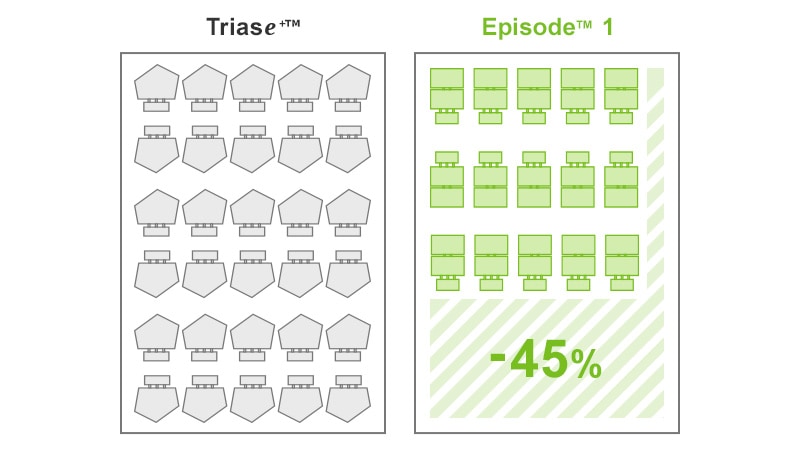
In addition to its high productivity, Episode™ 1 offers a reduced footprint. Compared with the Triase+™ series, twice as many smaller modules can be installed in a system. With the same number of modules installed, Episode™ 1 takes up about 45% less fab space than its predecessor.
Another advantage of Episode™ 1 is the upgraded system for equipment data collection and edge information processing, which has a large storage capacity and a powerful CPU that can collect and analyze a greater amount of data than before. The data exchange method has been upgraded from analog to digital for faster transmission. The system’s operation and energy consumption data are stored in a database and analyzed by a dedicated application to generate ideas for improving production efficiency and performance.
TEL’s Technologies Improve Everyday Life
The evolution of AI is seemingly unstoppable. We know that a PC is powered by a CPU, and the more cores a CPU has, the better it can perform, such as running multiple tasks simultaneously. Today, quad-core (4-core), hexa-core (6-core), and octa-core (8-core) processors are mainstream. Think of AI as a processor with an infinite number of cores, and you can imagine how powerful AI’s processing power can be.
The evolution of AI demands further scaling of semiconductor devices, which in turn requires systems capable of depositing films on tiny areas of ever finer device structures. To make better use of AI in everyday life, it will be necessary to accelerate the spread of AI to personal equipment, including smartphones. Smaller AI chipsets that fit into smartphones will be produced as further device scaling becomes feasible.
The use of Episode™ 1 will soon expand from logic to various other devices. The current application is for the deposition of titanium films on the inside of contact holes, but the processes are also being developed for other new materials that could further reduce contact resistance. These advances will eventually be applied to the production of full-fledged AI processors.
TEL has also introduced Episode™ 2 DMR (Duo Matched Reactor), which can transport and perform film deposition on two wafers simultaneously. As with Episode™ 1, the system offers high productivity and a small footprint.
TEL’s deposition systems powerfully support device scaling to help people live better lives.
Share
