Cryogenic Etching - Tokyo Electron’s “Digital and Green Transformation” of Semiconductor Process Equipment
Technology
The evolution of semiconductors will continue to be critical to the advancement of a wide range of industries. One of the driving forces behind the current evolution is 3D NAND flash memory, which enables larger capacity, higher speed, superior reliability, and lower power consumption.
In the 3D NAND field, Tokyo Electron (TEL) has developed a new HARC etch technology called cryogenic etching. In addition to productivity gains, the new technology can reduce CO2 emissions by 80% or more over conventional technology. It will make a significant contribution to industrial development in the future.
The article gives an overview of the current semiconductor market environment, what kind of technology innovation is required, and explains the benefits of cryogenic etching.
Evolution of Semiconductors is the Key to Technology Advancements
Technology is advancing at a dizzying pace, creating convenient digital devices such as PCs, smartphones, automotive electronics, and IoT home appliances, to name a few.
The growth of these devices and internet services/platforms has been led by the continued evolution of semiconductors. Often referred to as the “key in the industry,” semiconductors have played a vital role in supporting numerous industries and the global economy.
The evolution of semiconductors has enabled advances in computing technology, making it possible to process massive amounts of data increasingly faster. Semiconductors are already playing a critical role in a wide range of services that will drive the future society, including generative AI (such as ChatGPT), on-device AI, virtual reality, and self-driving vehicles, among others.
The semiconductor market is expected to grow to $1 trillion USD by 2030. It took the market 75 long years to reach the $500 billion USD, but in all likelihood it will take less than a decade to add another $500 billion USD.

This anticipated increase in the market provides TEL with an excellent opportunity to contribute to society through technological innovation. As a milestone, TEL has initiated the Medium-term Management Plan to ensure further growth, investing 1.5 trillion yen or more in R&D and 700 billion yen or more in capital expenditures over the next five years.
However, as the digital transformation of our society advances, there is a concern that the world will face an electricity shortage in a few decades if the current rate of growth in electricity consumption continues. To maintain the industry’s progress, it is vital to develop semiconductors with larger capacity, higher speed, superior reliability, and lower power consumption, while pursuing digital and green transformation on a global scale.

3D NAND Enables Greater Semiconductor Capacity and Faster Processing
A semiconductor called "NAND flash memory", which is to store data, is used in large quantities not only in everyday electronic devices such as smartphones, but also in data centers and other places. Initially, the structure had memory elements arranged in a planar direction. Since then, the semiconductor scaling has progressed to meet demands for larger capacity, but when it reached its limit, a new technology called 3D NAND, in which memory cells are stacked vertically, was invented.
Trend of technological innovation in NAND flash memory stacking

3D NAND has a revolutionary structure that allows for an increase in the number of layers, thereby increasing the memory density per device. However, another issue has become apparent: an increase in the number of layers led to a rise of manufacturing costs as well. What is needed is an etching technology that can process contact holes with a high aspect ratio*in a short amount of time, with high productivity. For example, if we can reduce a processing step that previously took three times to two, we can reduce manufacturing costs accordingly.
- aspect ratio: depth-to-width ratio of a pattern formed on a wafer

How challenging is the HARC etching technology for 3D NAND? This technology allows for the simultaneous and uniform drilling of approximately 2 trillion holes, each 8mm deep with the width of a human hair, in an area the size of the Tokyo Dome in just 33 minutes.
In response to this trend, TEL started developing a new etching technology around 2014. As die stacking of 3D NAND progresses, TEL released the cryogenic etching technology in 2023, making it possible to etch contact holes through more than 400 layers in a stack.
TEL’s New Technology Shapes the Future to Support 3D NAND Evolution
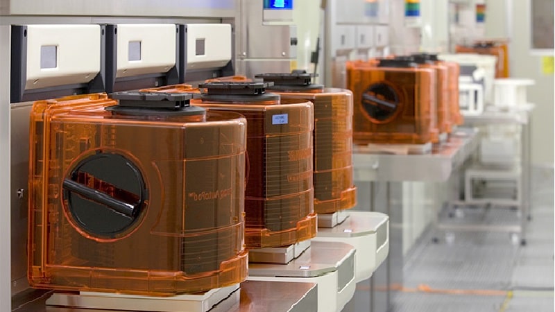
TEL's "cryogenic etching" is a new technology that uses an extremely low-temperature process of negative tens of degrees Celsius to achieve high-speed etching while also optimizing through machine learning.
In HARC etching, brines (antifreeze solutions) are passed through the plasma processing equipment to prevent overheating of the wafer. Conventional equipment uses brines at temperatures ranging from 0℃ to as high as 80℃, depending on the application. In contrast, cryogenic etching technology uses cryogenic brines reaching temperatures as low as negative several tens of degrees to keep wafer lower than ever before. With this technology, it is now possible to etch straight contact holes deeper than 10μm at a rate 2.5 times faster than previously. Because the fast etch rate is maintained over time, the technology reduces power consumption by more than 40% compared with before.
Another notable feature of the cryogenic etching technology is the non-use of CF (fluorocarbon) gases. Previous HARC etching technologies have typically used CF gases, which contain carbon (C) and fluorine (F). The problem was that CF gases have a high global warming potential (GWP). As the mainly used CF gases including C4F8 and CF3, can have a significant impact on the environment, there has been a global trend to switch to other plasma energy sources.
For cryogenic etching, hydrogen fluoride (HF) gas can be replaced with CF gas. The latest generation of cryogenic etch system has successfully replaced 91% of the CF gases with HF gas, achieving over 80% reduction in carbon footprint compared with the first-generation system, while providing equal or better processing performance. This is another feature of cryogenic etching that makes it essential to the digital and green transformation.
Environmental Performance Index Comparison

Behind TEL’s success in establishing this new technology is a corporate culture that values continuous investment in R&D and has an aspiration for new challenges. All of the engineers have persevered through numerous trials and errors, never giving up and continuing to make progress. The decade-long journey to achieve this new technology exemplifies our tenacity to win, fostered by an environment that encourages challenge.
Cryogenic etching technology will enable semiconductor devices to be produced faster and with less power, driving further advancing semiconductor and peripheral technologies, and the digital shift in society. Production readiness assessment is now underway, with low-volume production expected to begin in 2025 and high-volume production in 2026*. Following our presentation at academic conferences, more inquiries are coming from customers asking whether the technology could be extended to devices other than 3D NAND. In fact, the technology has tremendous potential to enhance the production of any device that requires etching.
- as of August, 2024
Accelerating Digital and Green Transformation
“Technology Enabling Life” is TEL’s corporate message. As the world’s leading companies increasingly address “Zero Emissions”, the manufacturers that supply the devices critical to their operations also need to improve their environmental performance. The market for semiconductor etch systems is steadily expanding, leading the growth of TEL’s business. In fact, our performance in this segment directly affects the overall evaluation of TEL.
Cryogenic etching technology is already taking the next step to accelerate the digital and green transformation of society. Currently, the technology can produce contact holes with an aspect ratio of 1:100 and multiple etch processes stacked vertically for even finer processing. Our next goal is to etch 1:200 aspect ratio holes in a single process. Once it is achieved, the industry will see further improvements in productivity and power consumption.
From a green transformation perspective, we will soon need to start replacing PFAS (per- and polyfluoroalkyl substances) in machine coolants and CFC gases in refrigerators. Developing the technology to ensure stable low-temperature processes while protecting the environment is not something that happens overnight. That is why we will continue to work hard and do research to deliver value to our customers.
Share
