A Plasma Researcher on TEL’s Inspiring R&D Environment
Technology
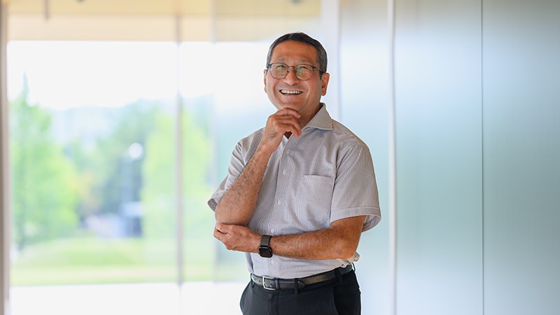
Plasma, known as the fourth state of matter after solids, liquids, and gases, is essential to the advanced semiconductor manufacturing processes behind the smartphones and computers we rely on every day.
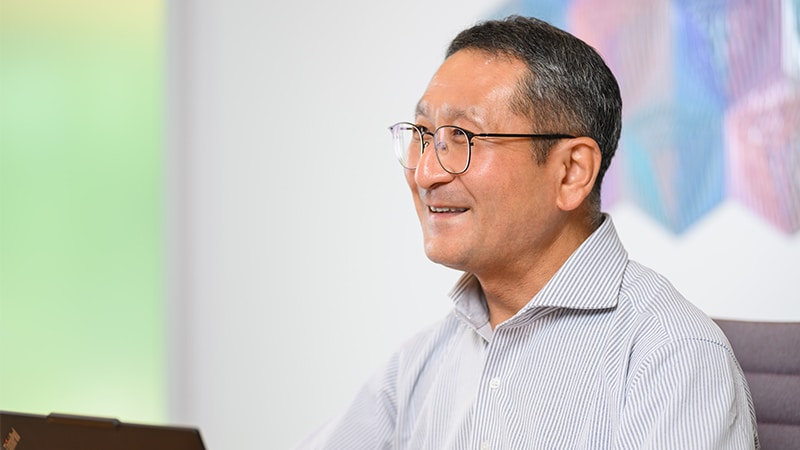
Yohei Yamazawa of Tokyo Electron Miyagi has spent more than 25 years studying plasma, dating back to his graduate school days. What motivates a researcher to pursue unanswered questions for decades and cherish moments of sudden insight? We spoke with Yamazawa about the depth and fascination of plasma research, and the unique appeal of conducting cutting-edge research at Tokyo Electron (TEL).
Profile
-

Yohei Yamazawa
Advanced Technology Solution Development Division
Conductor & CCP Solution Development Department
Chief Engineer / Plasma Scientist / Ph.D. in Human and Environmental Studies
Yamazawa joined Tokyo Electron in 1999 and has more than 30 years of experience in plasma research and development, including six years of graduate study. A specialist in RF*1 plasma systems, he has contributed to numerous technological advancements in semiconductor manufacturing. He also earned a Ph.D. while pursuing his career at TEL.
- RF: Radio Frequency
- CCP: Capacitively Coupled Plasma
Plasma Etching: Essential for Semiconductor Miniaturization
Could you briefly explain what plasma is and its role in semiconductor manufacturing?
Yamazawa
Plasma is a unique state of matter created by applying strong electrical energy to a gas, causing ionization that generates electrons and ions, which then move freely within the gas. While it may sound unfamiliar, plasma is all around us. The sun and fluorescent lamps are everyday examples of plasma.
In semiconductor manufacturing, plasma’s high reactivity is used to remove material from wafer surfaces and create extremely thin films. Put simply, it serves as a highly precise tool for fabricating semiconductor devices.
Specifically, at what stages of semiconductor manufacturing is plasma used?
Yamazawa
Plasma is mainly used in three key manufacturing processes. The first is etching, which is used to create circuit patterns by removing material.
Semiconductors are made by selectively removing unwanted portions of thin films deposited on a wafer, forming intricate patterns and structures. Today, some of the features being created require aspect ratios as high as 100:1. Conventional wet etching, which uses liquid chemicals, cannot produce such deep and narrow structures.
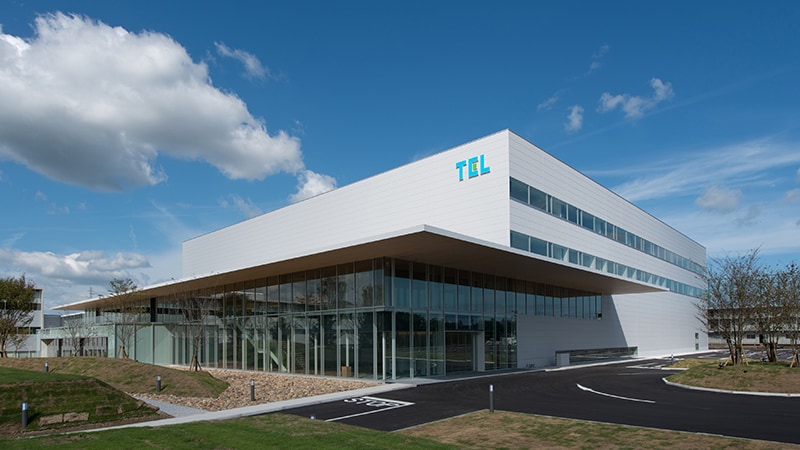
Only dry etching, which uses plasma, can precisely and vertically remove material from targeted areas of a film. Tokyo Electron Miyagi develops and manufactures plasma etching systems used for this process.
The second is film deposition, a process in which dozens of ultra-thin layers are stacked to form semiconductor structures. With many conventional deposition methods, the wafer must be heated to high temperatures. Plasma, however, enables thin films to be deposited without significantly increasing the temperature. This is a major advantage, as temperature changes can sometimes distort delicate structures and affect device performance.
The third is cleaning. Plasma is used to remove microscopic contaminants and unwanted residues left behind after processing, leaving the wafer clean and ready for the next manufacturing step.
The cost of semiconductor manufacturing is heavily influenced by processing efficiency. If a manufacturing process becomes ten times more complex and takes ten times longer to complete, the cost can increase by a similar factor. Plasma technology, however, can dramatically improve productivity. By making the most of plasma’s unique properties, etching rates can be increased by as much as 10 to 20 times. That is why plasma is such a critical technology for the continued miniaturization and performance improvements of semiconductors.
Plasma Etching Becomes Reality:
A Key Discovery by Japanese Engineers
How has plasma etching technology evolved over the years?
Yamazawa
Plasma etching has been studied since the 1950s, long before computers became a part of everyday life. Research continued for decades, and it was a Japanese engineer who first recognized its potential and helped pave the way for its practical application.
First, plasma contains ions and electrons generated through ionization, as well as highly reactive radicals that, while not ionized into ions, have absorbed energy and entered an excited state. Because ions carry an electric charge, they can be accelerated by applying a voltage. When they strike a surface, they remove material much like billiard balls knocking objects away, allowing highly directional etching along the path of the ions. However, the downside is that they can also erode the resist layer that is meant to protect areas that should not be etched.
Radicals, on the other hand, etch materials through chemical reactions. Although they lack the directional nature of ion etching, they can be controlled to selectively remove only the desired film while preserving the resist.
By combining the strengths of both ions and radicals, a synergistic effect can be achieved, enabling highly precise etching that removes only the target material, in the desired direction, and at speeds more than ten times faster than would otherwise be possible. This technology, known as Reactive Ion Etching (RIE), is also used in Tokyo Electron Miyagi's etch systems.
This phenomenon was discovered in 1973 by two engineers, Naokichi Hosokawa and Reisaku Matsuzaki, who were working at Nippon Electric Varian Ltd. (now Canon Anelva Corporation).
Their breakthrough laid the foundation for a technology that continues to play a vital role in semiconductor manufacturing today.[1][2]
So Japanese innovation played a major role in the development of this globally important technology.
Yamazawa
Absolutely. It was the application of this phenomenon that made economically viable microfabrication possible for the first time. Without this technology, semiconductors would not have continued to become smaller and more powerful, and the smartphones in our hands today might not exist. In terms of its impact on society, I believe this achievement is every bit as significant as many research breakthroughs that have received Nobel Prizes. It laid the technological foundation for the semiconductor devices that support modern life.
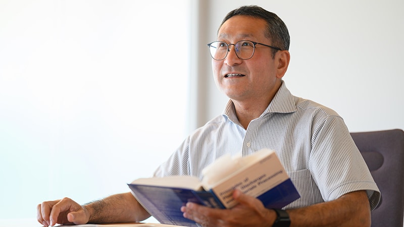
Interestingly, I did not learn about this until much later, around 2010. I had the opportunity to attend a lecture by Professor Lieberman,* who is well known for authoring one of the most influential books on plasma processing, at the Special Evening Session of the Gaseous Electronics Conference. During his presentation on the history of semiconductor processing, he explained that this technology had originally been discovered by Japanese engineers. I was surprised to hear the fact. today, our work builds on that discovery.
[1] https://eetimes.itmedia.co.jp/ee/articles/1809/28/news018_3.html
[2] https://www.shmj.or.jp/dev_story/pdf/develop27.pdf
[3] https://meetings.aps.org/Meeting/GEC10/Session/FT.1
[4] H. Abe, M. Yoneda and N. Fujiwara, ``Developments of Plasma Etching Technology for Fabricating Semiconductor Devices,'' Jpn. J. Appl. Phys. 47, 1435 (2008)
https://iopscience.iop.org/article/10.1143/JJAP.47.1435/meta
- Michael A. Lieberman, Ph.D., is a professor of electrical engineering at the University of California, Berkeley. He is best known as the author of Principles of Plasma Discharges and Materials Processing, a widely recognized textbook in the field of plasma science and engineering.

What Makes Plasma Research So Fascinating
Could you tell us about your career path? You’ve spent your career working with plasma, but how did you first become involved in semiconductor production?
Yamazawa
As a student, my research was more closely related to nuclear fusion. While fusion is one of the major applications of plasma, it is quite different from the type of plasma used in semiconductor manufacturing. What attracted me to the semiconductor industry was that it supports real-world industries and that new technologies can be put into practical use much more quickly. That gave me a more tangible sense of how technology could evolve and make an impact.
After graduating, I decided that the semiconductor industry would be the best place to continue working with plasma. Among the companies in the field, TEL stood out to me as a fast-growing and dynamic company, so I joined the organization. Fortunately, I was assigned to a role that matched my interests, and since then I have consistently worked on plasma diagnostics, control technologies, and plasma source R&D.
In 2001, with the support of my colleagues and mentors, I earned my Ph.D. while continuing to work full-time. Being able to immerse myself in my field of expertise led to opportunities such as filing patents as early as my first year at TEL.
Are there any research projects or challenges from your early career that stand out in your memory?
Yamazawa
One project that stands out was my work in my third year at TEL on understanding the mechanism behind harmonic generation.
One challenge I tackled during my third year at TEL was uncovering the mechanism behind harmonic generation in plasma. Plasma is typically generated by applying an RF electric field to an electrode, most commonly at 13 MHz. Yet, even when operating at exactly 13 MHz, frequencies at two or three times that value would sometimes emerge, affecting the behavior of the plasma. In some cases, something as simple as changing the length of a cable could alter the results. What puzzled researchers at the time was that no one fully understood why this was happening.
How did you go about researching the problem?
Yamazawa
I didn't limit my work to the lab or office during the day. I would print out data, take it home, and look through it whenever I had free time. At some point, I was no longer consciously analyzing the graph, but because I was thinking about the problem so intensely, all the necessary information stayed in my head.
My subconscious kept working on it. Looking back, I often felt that my ideas progressed not when I was sitting at my desk, but when I was relaxing in the break room or simply letting my mind wander. Those quiet moments were often when new insights emerged.
The turning point came on a Friday night. On my way home from work, I stopped at a restaurant and ordered a bowl of udon. While waiting for it to arrive, I found myself looking over
the data once again.
Then, all of a sudden, everything clicked. I realized that the puzzling phenomenon could be fully explained by changes occurring at integer multiples of 13 MHz. In that moment, it
felt as if a light bulb had gone on in my head.
As a researcher, that was the kind of experience you only have a few times in your lifetime. The answer to a problem that had seemed impossible to solve suddenly became clear, and all the pieces fell into place.
Once the idea came to me, I simply couldn't stop thinking about it. I was supposed to leave on a trip the next day, but instead of packing, I spent hours organizing my thoughts so I wouldn't forget them.
Compared with the discovery of Reactive Ion Etching mentioned earlier, it was a very small finding. But at that moment, I believed I had finally identified the cause of a phenomenon that had remained a mystery for a long time. For that brief moment, I felt that I might have been the only person in the world who knew the answer.
That may sound dramatic, but I remember thinking: what if something happened during the trip? This discovery might never be shared and could be lost forever. After sending my notes and data to my colleagues, I finally started packing. By then, dawn was just beginning to break.
That story really captures both your dedication to research and the excitement of exploring something no one has understood before.
Yamazawa
Fortunately, the knowledge we gained at that time is still being used today. The work also gave me opportunities to publish papers and present my findings at academic conferences.
I believe one reason I was able to take on such impactful research early in my career is TEL’s culture of listening. No matter how little experience you have, your managers and colleagues take your ideas seriously.If your research has real value and can make a difference, the company will support it.
Before joining TEL, I was worried about whether my research would be valued once I entered the professional world and whether I would be able to continue pursuing the topics that interested me. Looking back now, I feel that the value of your research is not something you wait for others to recognize. You demonstrate its value by delivering results.
At TEL, if you seriously pursue work that aligns with the company’s needs while also finding subjects that genuinely excite you, opportunities will come your way.

Technology Only Matters When It Is Put To Use
Tell us about the excitement of developing new technologies and bringing them into the world.
Yamazawa
Manufacturing companies take many different approaches to research and development. But one simple indicator of how seriously a company takes R&D is the percentage of its revenue that it invests in development. Across all industries, the average is about 3%. At TEL, however, that figure is around 10%.
I believe that is one reason why new technologies and fresh ideas are always valued here. The company actively encourages innovation and is willing to entrust important work to
younger engineers and researchers. As a result, people are given opportunities early in their careers to take ownership of challenging projects and contribute to the development of
new technologies.
Another reason is that the semiconductor industry moves at an incredibly fast pace. In the field of nuclear fusion, for example, the start of experiments at ITER, the International
Thermonuclear Experimental Reactor, has been postponed to 2033 or later. Had I remained in that field, I might have reached retirement before seeing the results of my work come to
fruition.
The semiconductor industry is different. New technologies move from research to real-world application much more quickly. That has given me the opportunity to see many of the
technologies I have worked on become actual products and make an impact in the world. There is great satisfaction in knowing that your research is being put to use and helping
advance an industry.
To me, technology is only meaningful when it is applied and creates value for society. What matters most is that it finds its way into products and contributes to their development.
Seeing equipment based on the harmonic generation principle I mentioned earlier lined up in a customer's cleanroom was especially rewarding. I even bought a game console made with chips produced using our technology, despite not being much of a gamer. I remember looking at it over a drink, feeling grateful that our technology was being put to use.
Finally, as a plasma researcher at TEL, what are your goals for the future?
Yamazawa
I currently serve as a Chief Engineer in a division developing next-generation equipment. With just four years remaining until retirement, I have recently found myself thinking about how many new challenges I can take on during the time I have left.
That said, TEL is a place where I can keep working on new ideas right up to the very end of my career. I am confident that there are still exciting discoveries ahead. With the time I have left, I want to make the most of every opportunity and continue pushing myself to do something new.
Share