


- Semiconductor Technology Now
Expert Interview
The Race to Develop SiC Power Devices Intensifies, The Real Test Will Be in the Next Five to Ten Years
March 31, 2015

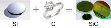
About 10% of electricity generated at power plants is dissipated in transmission before reaching appliances and personal computers at home. Typical culprits for these losses are the processes of voltage and frequency conversion. Reducing such losses is critical to attaining a sustainable society. The good news is that there is a type of device that can magically reduce the loss of electricity. The material used to build this device is silicon carbide, or SiC. Japan leads the world in the development of SiC-based devices, which are so promising that industries throughout the world are eagerly waiting for them to become available for a wide variety of applications. Telescope Magazine asked Professor Tsunenobu Kimoto, who leads the development of SiC devices at Kyoto University, about the current state and outlook of the development of this exciting device.
SiC power devices are a godsend
Telescope Magazine: How did SiC come to attract attention as a power device material that can reduce electricity losses?
Tsunenobu Kimoto: SiC has actually been studied for a surprisingly long time, and it was considered a promising semiconductor material several times in the past. After a technology for growing small pieces of SiC crystal was developed around 1950, the use of SiC in high-temperature semiconductor devices was vigorously explored in the 1960s and 1970s. And in the 1980s, SiC drew attention again as a material for blue light-emitting diodes (LEDs). Some SiC-based blue LEDs were actually produced and marketed in Japan and the U.S. None of these SiC booms lasted for long, however, because competing technologies proved superior each time.
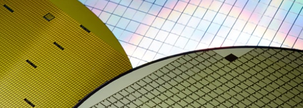
At Kyoto University, research into SiC power devices started in the early 1990s (Figure 1). SiC had been theoretically known to be an ideal material for power devices. Its physical properties are such that SiC-based power devices are potentially superior to silicon (Si)-based ones in terms of power losses, switching losses, and overall energy efficiency. Smaller power losses mean less heat generation, which translates into smaller power converters. Smaller switching losses also lead to smaller components for power converters. As SiC devices can operate in high temperatures, cooling mechanisms can be made smaller or even done away with.
At the time Kyoto University entered this field of research, few others were trying to develop SiC-based power devices despite their clear and indisputable advantages. Why? Because the material was so tough to process that the difficulty dwarfed the advantages.
|
 |
Contents
Cross Talk
Visiting Laboratories
Expert Interview
Topics
Report Series
- Motorization, Act II – The Age of Automated Driving

- How Society Will Change in the Digital Age
- Part 1
- What is Digitalization?

- Sports Technology Protecting Athletes and Providing Fairer Refereeing