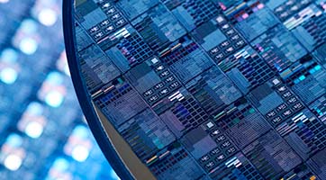


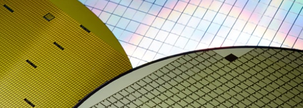
- Semiconductor Technology Now
Expert Interview
Scientific analysis of SiC-related phenomena is vital to advancing the technology
Telescope Magazine: How smoothly is the technology development proceeding?
Tsunenobu Kimoto: Both the crystal-making and interface issues are being addressed steadily, but only slowly. It suggests that basic research is still insufficient in this field.
We already know the rough physical properties of SiC. But there are many device simulation parameters we need to figure out in order to predict the device properties. Although the development efforts are ongoing vigorously by trial and error, we still don't know the underlying principles of many of the phenomena we encounter. Cultivating our scientific insights in this area will directly advance our technologies.
 |
Telescope Magazine: Just like SiC, gallium nitride (GaN) is considered to be a promising material for power devices. How do you think their respective roles are going to be?
Tsunenobu Kimoto: GaN devices will be used for power units with relatively low breakdown voltages at 200 V, 300 V, or 600 V. They will be particularly effective in low-current applications.
As for automobile applications, SiC devices are suitable for things like motor driver units that power electric vehicles. In contrast, GaN devices will suffice for lesser applications like DC voltage converters that turn the car battery power to 48 V for onboard equipment, because these applications only require a low breakdown voltage of 200 V and a low current of 10 A or 20 A. Since this domain is not the forte of SiC or Si devices, GaN can be complementary to these materials.
Telescope Magazine: What SiC applications other than power devices do you have in mind?
Tsunenobu Kimoto: High-temperature semiconductor devices will be worth developing, although the market size will not be as large as that of power devices. With such semiconductors, electronic circuits can be made to operate at 300 degrees Celsius or so, including memory units. That could open up applications in such areas as high-temperature components of a car or resource mining equipment. Notably, NASA in the U.S. is developing space-use SiC devices. SiC-based integrated circuits (ICs) used to be an unreachable dream, but they've already become a reality, at least in laboratory settings.
Associate Professor Jun Suda, who is a member of my laboratory, is building MEMS, or micromachines, using monocrystalline SiC for cantilevers. Because SiC is hard, the resonance frequency of a device can be made higher, which delivers stunningly superior sensitivity when used in temperature or pressure sensors. SiC-based microsensors can operate at high temperatures, and may be coupled with an SiC-based IC.
Developers' competition intensifies as market's expectation rises
Telescope Magazine: Since SiC devices are the key to improving energy efficiency of various systems, the priority of their development must be rising steadily.
Tsunenobu Kimoto: The competition among the developers will certainly intensify. Until recently, Japanese companies and research institutions have competed mainly with their counterparts in the U.S. and Europe. Japan is slightly ahead of the others in terms of technologies for producing SiC crystals and devices. When it comes to production technologies, however, we are not necessarily a leader.
And Asian players including China, Korea, and Taiwan are sure to accelerate the pace of development to close the gap. If Japan is to maintain its lead, we need to pursue basic research and deepen our understanding of the underlying science.
To take a lead in the SiC business, packaging and module technologies will also be essential. Current SiC device packaging is modeled on Si-based technologies, but if we take advantage of SiC's properties, it will be possible to achieve even higher packaging density, so that's what we need to work on.
I think the next five to ten years will be the real test for us.
 |
The contents of the article is at the time of announcement.
Profile
Tsunenobu Kimoto
Professor of Electronic Science and Engineering at the Graduate School of Engineering, Kyoto University
Born in 1963, Kimoto completed the master's course at the Graduate School of Engineering, Kyoto University in 1988, and joined Sumitomo Electric Industries the same year to pursue research into amorphous and diamond semiconductors. In 1990, Kimoto became an assistant at the Faculty of Engineering, Kyoto University to commence studies of SiC semiconductors, receiving his engineering doctorate in 1996 for his studies on crystal growth, physical property assessment, and diodes with high breakdown voltages. After serving as a guest researcher of physics at Linköping University in Sweden from 1996 to 1997, he became an assistant professor at Kyoto University in 1998 and subsequently professor in 2006. He was a core researcher in the Funding Program for World-Leading Innovative R&D on Science and Technology (FIRST) sponsored by the Cabinet Office from 2009 to 2014, and became the chair of the Advanced Power Semiconductors Division at the Japan Society of Applied Physics in 2014. Throughout his career, Kimoto has pursued basic research related to SiC power semiconductors, including crystal growth, physical property analysis, defect electronics, ion implant and MOS interface control, Schottky barrier diode, PiN diode, MOSFET, JFET, BJT, and IGBT. He is also pursuing such basic research interests as the state of electrons and carrier transport in semiconductor quantum wires, resistive random access memory, and GaN power devices.
Writer
Motoaki Ito
Motoaki Ito is the CEO of Enlight, Inc. which he founded in 2014. The company leverages its expertise in communicating the value of specific technologies to the target, and offers marketing support mainly to technology companies. Prior to setting up Enlight, Ito worked for Nikkei Business Publications (Nikkei BP) for four years as an advertising producer of its technology information group, with a main focus on marketing support. Before that, he spent six years as a consultant at TechnoAssociates, Inc., a joint think tank between Nikkei BP and Mitsubishi Corporation, supporting the clients' manufacturing operations. Prior to that, he worked for 12 years as a journalist, editor, and editor-in-chief for various publications including Nikkei Microdevices, Nikkei Electronics, and Nikkei BP Semiconductor Research, after a three-year stint at Fujitsu developing semiconductors as an engineer.
Contents
Cross Talk
Visiting Laboratories
Expert Interview
Topics
Report Series
- Motorization, Act II – The Age of Automated Driving

- How Society Will Change in the Digital Age
- Part 1
- What is Digitalization?

- Sports Technology Protecting Athletes and Providing Fairer Refereeing