


- Semiconductor Technology Now
Expert Interview
Higher breakdown voltage and higher current density required
Telescope Magazine: What kinds of SiC devices need to be developed to expand their application?
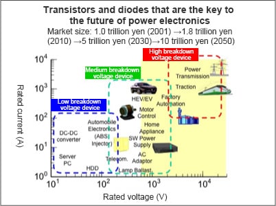
Tsunenobu Kimoto: To broaden the application of SiC devices, they must be made to withstand higher voltage and handle higher current (Figure 5). The breakdown voltage of a semiconductor device is determined by its thickness, and the amount of acceptable current is determined by its surface area. The thickness issue can be overcome without major obstacles. We have already developed an SiC transistor with a breakdown voltage of 20,000 V (Figure 6). Power supply units for home appliances are in far greater demand, and they only require a breakdown voltage of 600 V with 100 V AC power supply, or 1,200 V with 220 V AC power supply. So, the bar is much lower with home appliances than with railroad applications that have already been successfully implemented.
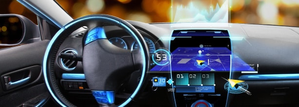
As for electric current, automobiles and other large-volume applications require SiC devices that can carry a large current. The currently available SiC devices can only handle up to 20 A, but motor driver circuits for electric vehicles and hybrid cars need devices that can carry 100 A or 200 A. With railcars, power devices are used in parallel to handle large currents. But this solution does not work with automobiles because cutting production cost is a must in this industry. That is why we are working to develop SiC chips that can handle 200 A singly or in a pair.
 |
Telescope Magazine: What sort of improvements does the current technology need?
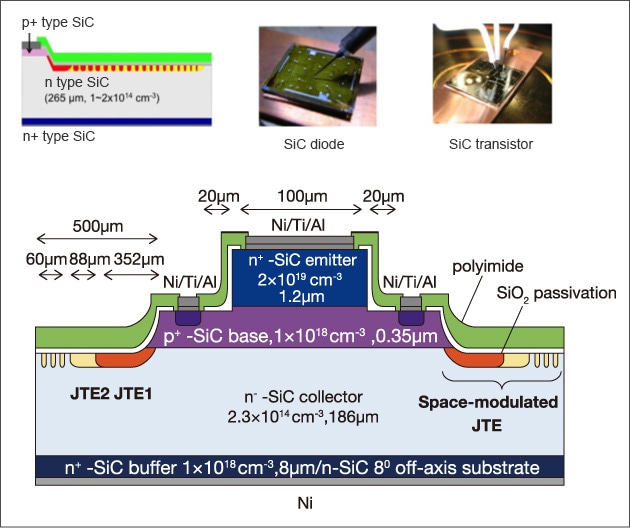
Tsunenobu Kimoto: There are two points to cover. One is to produce large SiC crystals of higher quality, which directly affects the device yield. At present, the production yield of power devices using 1 mm2 SiC crystal chips is over 90%, and that of devices using 3 mm2 chips is 70 or 80%, which is good enough for business. But when the chip size exceeds 5 mm2, the yield starts to plummet. To manufacture 10 mm2 chips that can withstand a current of 200 A while maintaining a production-worthy yield level, the crystal defect rate has to be reduced by an order of magnitude.
Telescope Magazine: And what's the other point?
Tsunenobu Kimoto: Within the transistor channel that controls the current, the quality of the interface between the oxidized film and the semiconductor material has to be further improved. That would be crucial to building a MOS structure with good properties and reliability. The MOS structure has been credited for making Si devices the current mainstream. Unfortunately, no one has succeeded yet in producing the SiC interface as clean as the Si interface. Oxidation films made with thermal oxidation are good insulators, but there are so many interface defects that SiC transistors just cannot demonstrate their true potentials. The electron mobility (a measure of an electron's ease of movement) in Si devices is 400-500 cm2/Vs. The innate physical property of SiC being as it is, the electron mobility in SiC devices can be theoretically as high as 300 cm2/Vs, but the real-world figure is minuscule at about 20 cm2/Vs.
It is conjectured that the poor interface quality of SiC comes from residual carbon (C), but because detecting C on the interface is so difficult, the mechanism of the deterioration of interface quality remains unknown. But the chip area can be made smaller once the electron mobility reaches 100 cm2/Vs, so all we need is one more push in that direction.
 |
Contents
Cross Talk
Visiting Laboratories
Expert Interview
Topics
Report Series
- Motorization, Act II – The Age of Automated Driving

- How Society Will Change in the Digital Age
- Part 1
- What is Digitalization?

- Sports Technology Protecting Athletes and Providing Fairer Refereeing