- Semiconductor Technology Now
Science Report
Past, Present, and Future of Moore's Law, which Supports the Advancement of the Semiconductor Industry
- June 2, 2021
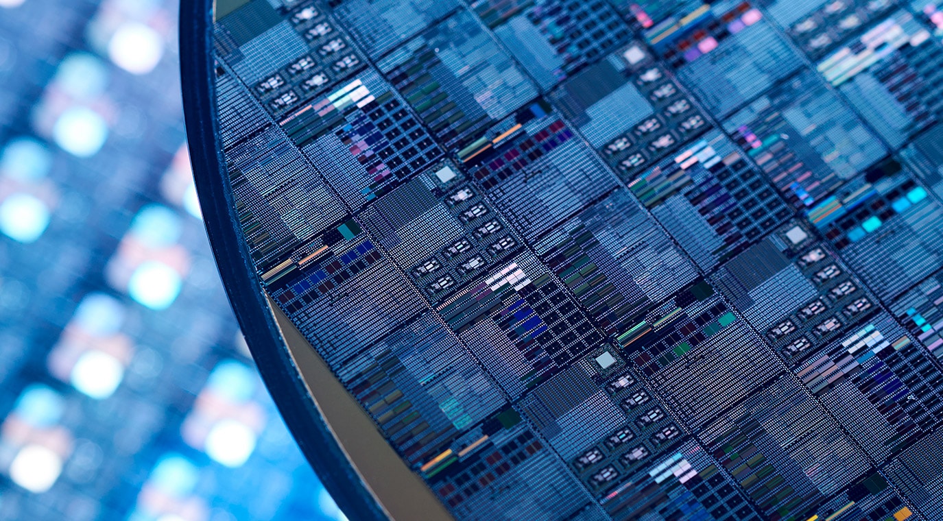
The empirical rule driving the development of the semiconductor industry over at least the past half-century is Moore's Law. Semiconductors have achieved astonishing development through increasing integration levels along Moore's Law and falling costs (reductions in cost per transistor formed on an integrated circuit (IC)), vastly altering the appearance of electronic instruments that contain these semiconductors and the society that utilizes them. In addition, Moore's Law has been functioning as an absolute anchor for industry people working at companies manufacturing semiconductor manufacturing equipment, materials, devices, and electronic instruments, as well as service providers, helping them to implicitly plan for predetermined harmony.
Despite the fact that it has been repeatedly declared that Moore's Law has reached its limit due to economic, technical, physical, and other factors, the law has tenaciously continued to survive. Although the death of the law was talked about recently, EUV lithography, which is considered the ultimate lithography, has finally been commercialized, extending the life of Moore's Law further. Nevertheless, since atoms cannot be scaled further, two-dimensional scaling will eventually reach its limit, but some ICs continue to increase integration levels by moving to three dimensions. In the future, 3D technology will also reach a strength limit, like skyscrapers do, and Moore's Law might reach its death unless some ingenious scheme appears. However, even if it dies, the semiconductor industry will be freed from the spell of Moore's Law and continue to develop further toward the future, based on free-thinking.
This column explains Moore's Law from its birth to the world after its death along this flow.
Understanding the Original Text of Moore's Law
First, let's read the original text of Moore's Law to understand it correctly.
Gordon Moore (Figure 1) founded Intel Corporation (U.S.) in 1968, together with Robert Noyce, known as the inventor of the integrated circuit. Before that, in 1965, when he was the director of research and development responsible for integrated circuits at Fairchild Semiconductor (U.S.), Moore was asked by a magazine devoted to electronic technology*1 to write an article. Since he was in a position to promote sales expansion of little-known integrated circuits, which had been launched in the market only three years earlier, he wrote an article titled, "Cramming more components onto integrated circuits (Figure 2)." Moore later became the CEO of Intel, and because the company became the so-called patron saint of Moore's Law, many people mistakenly think that he proposed Moore's Law while at Intel. However, it was actually a "product" created during his days at Fairchild Semiconductor, a division of Fairchild Camera and Instruments located on the east coast of the U.S. (Figure 2).
Using two graphs in his article, Moore tried to explain that the recently launched integrated circuits were promising electronic devices that, in the future, would dramatically increase the number of components they contained.

- Figure 1. Gordon Moore
- Source: Intel press kit
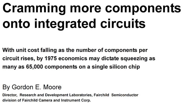
- Figure 2. Title and lead paragraph, with author's name and affiliation, of the article written by Gordon Moore describing the empirical rule that would later come to be known as "Moore’s Law”
- Source: Intel Newsroom
Integration level will keep doubling every year
A summary of the article follows.
“The complexity for minimum component costs has increased at a rate of roughly a factor of two per year. Certainly, over the short term, this rate can be expected to continue, if not increase. Over the longer term, the rate of increase is a bit more uncertain, although there is no reason to believe it will not remain nearly constant for at least 10 years.” He speculated that the number of components per integrated circuit for minimum cost would reach 65,000 by 1975 and concluded with the hopeful observation, “I believe that such a large circuit can be built on a single wafer.”
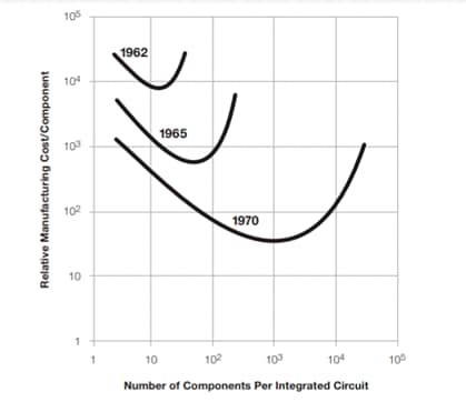
- Figure 3. Double logarithmic graph showing the relationship between the relative manufacturing cost (vertical axis) per electronic component contained on an integrated circuit in various years (vertical axis) and the number of electronic components contained in an integrated circuit (horizontal axis)
- Source: Intel Newsroom
Moore predicted that there would be an optimum number of electronic components per integrated circuit for minimum manufacturing cost and that technological progress would keep increasing this number every year. If you increase the integration level by cramming too many electronic components, the number of defects will increase and end up lowering the manufacturing yield (percentage of acceptable products), in turn increasing the cost per electronic component. Conversely, if the number of components is too small, the cost per component will end up increasing. What he most wanted to say was that the number of components per integrated circuit for minimum manufacturing cost would rapidly increase as time went on, i.e., in step with technological progress.
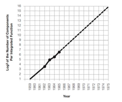
- Figure 4. Number of electronic components contained in an integrated circuit in each year (the dotted line indicates predictions)
- Source: Intel Newsroom
Figure 4 shows the famous semilogarithmic graph that became the basis for advocating Moore’s Law. In 1965, Moore plotted the number of components on only four types of ICs that Fairchild Semiconductor had been manufacturing and selling. They were all commercial integrated circuits containing the number of components that minimize cost, shown in Figure 3.
Moore boldly extrapolated the line in the semilogarithmic graph, obtained from just four points, by 10 years to 1975. This line means that the number of components contained in an integrated circuit will double every year. This is the empirical rule that in later years came to be known as Moore’s Law. There was no theoretical basis behind it; it was merely a prediction based on only 3 years of experience following the debut of integrated circuits in the world.
According to Moore’s recollection, the reason for extrapolating to 10 years out was because the magazine’s editorial department asked him to predict the future of the electronics industry over the next ten years, and it seems that he did not make it his 10-year prediction with much confidence. What made him make such a bold prediction?
Back then, discrete transistors were still in their heyday, and since any electronic circuit could be configured using only discrete transistors without using expensive integrated circuits, there was a widespread attitude that consumer applications didn’t need costly ICs. Thus, the use of ICs was limited to only some applications, such as cost-unconscious military uses. Therefore, because Fairchild Semiconductor needed to promote ICs and expand their sales, he wrote the article mostly to advertise the promise of semiconductors. Moore later recalled that he was not that confident about his prediction.
At the end of the article, he advanced his prediction further, saying, “Because the cost of electronic instruments will fall greatly thanks to reductions in cost per electronic component through higher integration levels, integrated electronics will make electronic techniques more generally available throughout all of society.” As specific application examples of ICs, he listed home computers or at least terminals connected to a central computer, automatic controls of automobiles, and personal portable communication equipment. A cartoon was added, depicting a crowd gathered at a counter selling hand-held home computers, which at that time were only possible in dreams. Back then, each corporation had only a single large computer called a “mainframe,” and it was an era when semiconductor memory had not yet appeared. More than half a century ago, Moore provided descriptions that hinted at the emergence of personal computers, autonomously driven cars, and smartphones, and his foresight is astonishing when one re-reads these descriptions now.
Corrected to “Integration Level to Double Every Two Years”
At the end of 1975, 10 years after he had written this article, Moore reexamined the trends in the integration level of ICs over the preceding 10 years and made a correction to “In the future, the integration level of semiconductors will double every two years.” From then on, this prediction came to be called “Moore’s Law,” which became an absolute anchor for people involved in semiconductors and the electronics industry. This empirical rule is generally known as the expression “The integration level of semiconductors doubles about every 18 to 24 months (one and a half to two years),” but Moore says he does not remember mentioning 18 months. Confusion may have been caused by the fact that the performance of Intel’s MPUs had been doubling every 18 months. There is also a historical background of the people involved in the memory business preferentially using the “doubling in 18 months” expression because the growth rate in the storage capacity of Dynamic Random Access Memory (DRAM), which had been quadrupling every three years over a quarter of a century since 1970, is equivalent to “doubling every 1.5 years (18 months).”
Moore’s Law, which Has Survived for More than 50 Years
In 2015, Moore’s Law hit its 50th anniversary since it was originally suggested. Over these 50 years, semiconductors have achieved astonishing advances through scaling, higher integration, and cost reduction according to Moore’s Law, and, as predicted by Moore, electronic instruments using semiconductors have made a more comfortable life and more efficient businesses a reality.
Back when Moore’s Law was suggested, the integration level was defined as the number of electronic components, including resistors, etc., contained in an IC. However, since transistors came to account for most of the electronic components as the integration level increased, Moore’s Law somehow came to be defined using the number of transistors contained in an IC.
The integration level of ICs has been increased by shrinking the gate width of MOS transistors and shrinking the circuit line width for about the first 40 years. Moore’s Law was declared dead every time scaling became difficultReference 1. However, coming into the 21st century, innovations were made to improve performance by drastically changing the transistor structure and constituent materials, thereby extending the life of Moore’s Law.
Several examples of changes in the transistor structure and constituent materials, which extended the life of Moore’s law, are described below. The planar structure*2, which had been in use since the time of IC invention, was replaced by the FinFET structure*3, which made it possible to suppress the leak current between the source and the drain, improving the current-driving capability. The insulating film/gate materials were also changed from the conventional SiO2/SiN (silicon nitride insulation film)/poly Si (polysilicon) gate to a high-k (high relative dielectric constant) insulating film/metal gate, suppressing the gate leak current. The wiring material was also changed from conventional Al to Cu, possessing high electrical conductivity, and Co and Ru will also begin to be used in the future. Lithography, which is the key technology for microfabrication, has been increasing the resolution level by shortening the wavelength of the light source used, from g-line (436 nm) to i-line (365 nm), to KrF (248 nm), and then to ArF (193 nm). Furthermore, the introduction of ArF liquid immersion lithography, which uses ArF excimer laser as the light source and water as the emersion liquid between the lens and the wafer, has improved the resolution level. Subsequently, extreme ultraviolet (EUV, at 3.5 nm) lithography using soft X-ray, which many people had considered impossible to implement, was put into practical use, opening a path toward shrinking logic devices beyond 7 nm, ensuring that Moore’s Law will live on further. This new technology will also be applied to cutting-edge DRAM (1α-nm products, i.e., 10-nm class fourth generation) starting this year, and its application is expected to expand.
Let’s look at an overview of how semiconductor devices have been following Moore’s Law in increasing the number of transistors over the past 50-plus years (Figure 5).
According to a survey by IC InsightsReference 2, a U.S. semiconductor market research firm, while the growth rates for some categories of products have declined somewhat, three-dimensional transition has begun for other devices Reference 3 as described below, and the transistor count per chip continues to double every two years even now, making Moore’s Law the guideline worth following for the semiconductor industry Reference 2.
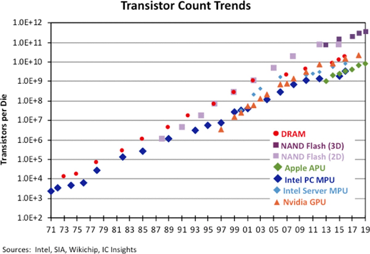
- Figure 5. Trends in the number of transistors contained in a semiconductor chip by semiconductor device type
- Source: IC Insights
Annual growth in NAND flash memory capacity remained at 55-60% through about 2012 but has since been around 30-35%. The shrinking of two-dimensional structures was stopped at 20 nm or slightly smaller, and in the case of NAND memory, the momentum for increasing the capacity is being restored by transitioning to three dimensions ahead of other devices, as described later. Already in cutting-edge products, the number of layers in three-dimensional structures has increased from 128 to 176.
The transistor count in DRAM used to increase at an approximate average annual rate of 45% until the early 2000s but subsequently declined to approximately 20% until the 16-gigabit generation, which appeared in 2016. The fact that there was less demand for capacity increases in DRAM memory than before was also one of the reasons for the decline. There were times it was thought that scaling would end at about 20 nm or slightly less, but EUV lithography has appeared as the savior and will be applied to DRAM, following logic devices, commencing the production of 1α-nm*4 products this year at long last.
The transistor count in Intel microprocessors (MPU) for PCs had been increasing at an average annual rate of approximately 40% until 2010. Since then, the rate has fallen by half. Although transistor count increases for Intel’s MPUs for servers temporarily paused between the middle and latter part of the 2000s, it has since begun to increase again at an annual rate of approximately 25%. Intel got tripped up many times in its effort to shrink circuit line width to less than 10 nm and decided to outsource production of some of its cutting-edge CPUs to TSMC (Taiwan). The company is now focusing on packaging technologies to increase integration levels by moving to three-dimensional structures.
Since 2013, transistor counts for Apple’s A-series application processors (APU) used in iPhones and iPads have continued to increase at the annual rate of 43%, up to the A13 processor containing 8.5 billion transistors, making the company the world leader in terms of scaling.
The high-end GPU from NVIDIA (U.S.) contains more transistors than other companies’ processors, already exceeding 50 billion, and has been increasing the integration level following Moore’s Law.
Based on the result of its recent analysis, IC Insights states, “The powerful drive of the IC industry to innovate its way over and around technology barriers can never be underestimated, but there are some very dramatic shifts underway regarding how ICs are designed and manufactured. Though some roadblocks standing in the way of progress toward future generations look more like high walls than hurdles, Moore’s Law continues to hold for the total IC industryReference 2.”
Only Three Companies Have Survived the Scaling Competition
Let’s look at the trends in semiconductor companies from the scaling viewpoint. Because process development costs and capital investment costs kept skyrocketing as circuit patterns were shrunk, semiconductor companies began to leave the competition one after another. Around 2002/2003, there were 26 semiconductor companies worldwide capable of manufacturing 130-nm devices. However, the number of companies continuing with scaling competition decreased. For example, there were only 18 companies at 90 nm and only 14 companies at 45 nm. Beyond 10 nm, only Intel, Samsung, and TSMC remained. In 7-nm processes*5, it seems that Intel and Samsung had been having manufacturing yield problems in their cutting-edge processes, including EUV lithography, for a long time, but industry sources say that Samsung has pulled ahead and is monopolizing outsourced production from cutting-edge fabless semiconductor companies.
Most Japanese companies stopped scaling at around 45/40 nm, and even Panasonic, which kept going with scaling until it became the only remaining company, also decided that scaling beyond 28 nm was meaningless because performance could not be improvedReference 3. This way of thinking might have been correct if the transistor structure and constituent materials had stayed the same. However, transistor materials, as well as structure, have changed completely, and more recently, EUV lithography, which had been considered impossible to implement, was put into practical use in some cases, dramatically improving the resolution of aligners and opening the path to further scaling.
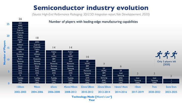
- Figure 6. Changes in the surviving semiconductor companies in each generation of scaling (company names in alphabetic order)
- Source: Yole Développement, a French semiconductor market research company
In the future, the transistor structure will evolve from FinFET to Gate-All-Around, in which the channel region is surrounded by a gate, suppressing the leak current and increasing the gate’s current driving power. For the channel region, germanium (Ge) and group III-V compounds that are selectively and epitaxially grown on silicon will be used in place of silicon and strained silicon. These channel materials have greater carrier mobility than silicon, enabling high-speed transistor operation. High-NA EUV aligners with N=0.55 possessing higher resolution than conventional EUV aligners with NA=0.33 are being developed toward commercializationReference 4.
Emergence of high-NA EUV and 2D materials extending Moore’s Law beyond 1 nm
Furthermore, two-dimensional materials are being researched as transistor channel materials in 1-nm processesReference 5. These are two-dimensional (2D) atomic layer, inorganic nanomaterials, such as graphene and transition metal dichalcogenides. Imec, a cutting-edge semiconductor research organization in Belgium, maintains that these new technologies and materials can now be expected to extend Moore’s Law beyond 1 nmsReferences 4, 5.
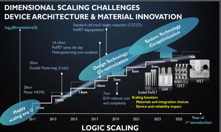
- Figure 7. Imec’s scaling roadmap for semiconductor logic devices
- Source: Imec
Figure 7 shows Imec’s roadmap for scaling logic devices. The vertical axis shows the transistor count per $1 in manufacturing cost, while the horizontal axis shows years. Down to around 28 nm, integration was achieved according to Moore’s Law by merely shrinking the conventional structure proportionally. However, Imec claims that to extend the life of Moore’s Law beyond that point, it will be necessary to develop a methodology that simultaneously optimizes IC design and process technology and which also simultaneously optimizes three elements—process technology, IC design, and system design. Imec, as well as semiconductor manufacturers, are aiming to extend the life of Moore’s Law through these simultaneous optimization methodologies.
However, when scaling arrives at the so-called “Atoms cannot scale” stage, physical limits will eventually be reached. Nevertheless, no one knows about the future that far out at present. There are even some people engaged in disruptive research in an effort to have molecules and atoms acquire memory effects and transistor effects.
Moore’s Law 2.0 for moving from 2D scaling to 3D stacking
Although many people mistakenly think that Moore’s Law is related to scaling, it is actually a law related to integration (number of transistors contained in an IC). Of course, since scaling increases the integration level per unit volume, it is certainly a powerful method. Even if planar scaling becomes impossible, that will not mean Moore’s Law is dead. If circuits are stacked three-dimensionally, the integration level per unit area will increase, further extending the life of Moore’s Law. The integration level is going to be increased vertically from now on. Some people refer to this shift to 3D to increase the integration level as “Moore’s Law 2.0.”
As for 3D packaging, memory devices have entered the implementation stage ahead of logic devicesReference 6. NAND flash memory has been the first to shift to 3D. All manufacturers have given up on scaling after the 20 to 15-nm*6 generations currently being mass-produced and are shifting to the direction of increasing the bit density per unit of chip area by three-dimensionally stacking memory cells. The resulting product is the so-called “3D NAND.”
Toshiba was the first company in the industry to propose the concept of 3D NAND in 2007. Using an etching process that pierces through all of the multiple stacked layers from top to bottom, multiple layers of memory cells are formed in a single step. This can drastically reduce the manufacturing cost compared to processes that form one layer of memory cells at a time.
In terms of mass production, South Korea’s Samsung Electronics has pulled ahead. In 2013, the company succeeded in mass-producing a 24-layer, 128-gigabit product using 2 bits/cell multi-value technology. Currently, companies are focusing on mass-producing 128-layer 3D NAND memory, and some have even commercialized 176-layer products. Before long, the number of layers will exceed 200.
In addition to flash memory, companies appear to be secretly conducting research on 3D DRAM but have not yet reached the commercialization stage. Instead, 3D packaging has been implemented that stacks and interconnects multiple completed DRAM chips using through-silicon vias (TSVs)Reference 6. DRAM modules, in which multiple DRAM chips and controller chips are stacked and connected using multiple TSVs, have been commercialized for use in high-end network equipment and supercomputers.
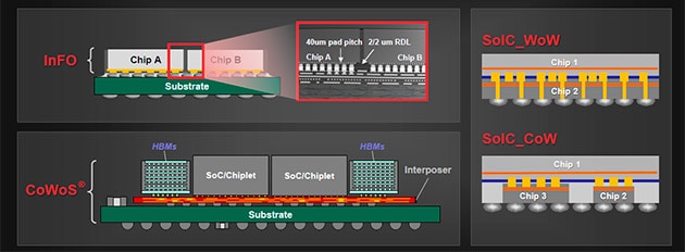
- Figure 8. Example of “system integration” in which multiple chips are packaged on a substrate instead of conventional chip integration
- Source: TSMC
As for logic devices, manufacturers are moving away from so-called chip integration, in which the integration level is increased within a single chip. Instead, system integration that integrates multiple semiconductor chips or chiplets (called “tiles” by Intel), into which conventional SoC chips are divided according to function, on a package substrate, is becoming the mainstream. Configuring a system by arranging chips in proximity of each other on a silicon interposer*7 provided on a substrate is sometimes called 2.5D packaging (examples are shown on the bottom left of Figure 8 and Figure 9).

- Figure 9. I-CUBE4 device, in which four high bandwidth memory (HBM) chips and a single logic chip for signal control are 2.5D-packaged on a silicon interposer, and which Samsung Electronics began shipping on May 6, 2021
- Source: Samsung Electronicss
Now, I will introduce the standard system integration methods of TSMC, which has many fabless companies and integrated device manufacturers (IDMs) around the world as customers. The first is InFO*8 (top left in Figure 8), which is characterized in that the silicon die has an extended outer area for connecting the package input/output pins. Having this outer area has made it possible to connect more than 1,000 input/output pins and also achieved bonding of multiple dies. The high-density re-wiring layer for rerouting input/output signals from the silicon die’s input/output pads to the package’s input/output pins is called the “Redistribution Layer (RDL)” and is formed using a thin film process.
The second method is CoWoS*9, which provides an intermediate silicon substrate called the “interposer” having multi-layer wiring formed in it on a packaging substrate made of resin, and arranges multiple silicon dies on the interposer in side-by-side proximity (bottom left in Figure 8).
More recently, the more difficult SoIC (System on Integrated Chips), which builds a system using Chip Stacking*100 and Wafer Stacking*11, has been developed. SoIC can be further classified into CoW (Chip on Wafer) and WoW (Wafer on Wafer) (right side of Figure 8). In an SoIC structure, multiple semiconductor chips (or wafers) can be stacked using bumpless interconnects, making it possible to transmit signals from one chip to another over the shortest distance. A 3D IC, in which more than 10 wafers are stacked, is also being developed.
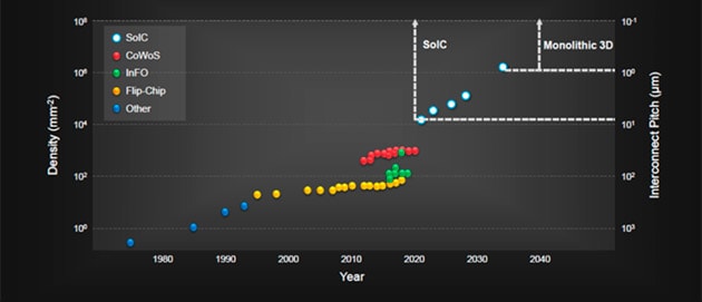
- Figure 10. History and future projection of the device input/output (I/O) densities and the interconnect pitch, achieved using various packaging technologies
- Source: TSMC
Figure 10 shows the history and future projection of the device input/output (I/O) densities and the interconnect pitch achieved using various packaging technologies at TSMC. Since 2011, TSMC has been increasing system integration density by applying CoWoS to many devices. In the future, the company says it is planning to dramatically increase the I/O density by stacking multiple chips vertically using 3D IC. The ideal monolithic 3D structure (an IC structure in which process technology is utilized to stack transistors on a single silicon substrate instead of stacking multiple silicon substrates), which was suggested a long time ago, is ultimately expected to be realized, but its materialization will likely take a long time.
Post-Moore’s Law: Start of a new era of striving for creative solutions
When 2D scaling reaches its physical limit in the so-called “Atoms cannot scale” stage, and the approach of increasing the integration level by stacking chips vertically using three-dimensional structures also reaches a limit in terms of strength, Moore’s Law will eventually die unless some new, ingenious schemes are developed.
If Moore’s Law stops working and this trend that has continued for more than half a century collapses, it will mean a shift from an era of using brute force to find solutions to a non-contiguous era in which wisdom and creativity will play the leading role.
If we regard the collapse of the scaling trend not as the arrival of an uneasy era with an uncertain future but as the arrival of an era of knowledge creation freed from the spell of chasing trends, it will also be possible to create a bright future with infinite possibilities. That is, an era will arrive when bold ideas based on creativity can send new, value-added products out into the world.
There will no longer be indexes and an evolution axis that restrict free-thinking, and it will be necessary to think of ways to improve system performance without relying on scaling. New movements have already begun, such as non-von Neumann architecture*12 that is different from the conventional von Neumann type.
The area that will be most severely impacted when Moore’s Law is dead will be semiconductor design. This means that designers who until now were preoccupied with developing products to which value is added through manufacturing or designing their implementation while in a sense riding free on Moore’s Law will be forced to develop products with added design-derived values. It will become clear that the semiconductor industry is a knowledge-creation type of industry, and the creativity of design engineers will be put to the test more than before.
Providing comfortable lifestyles in a sustainable society will become the keystone for future technology development. If I am asked to name a significant index directly linked to semiconductor characteristics, one that measures ultra-low power consumption for conserving energy comes to mind. When the full-fledged age of IoT arrives, in which everything is linked to the Internet and controlled from mobile devices, a shift to extremely ultra-low power consumption and energy conservation will be required.
Will the “Law of doubling energy efficiency every two years” replace Moore’s Law?
Nations around the world have set out toward decarbonization, and the demand for improving the power efficiency of semiconductor devices is heightening more than ever, especially with respect to reducing the power consumption of data centers. In his keynote address at ISSCC 2021, TSMC’s Chairman Liu said, “IC’s energy-efficient performance (throughput × throughput/Watt) will continue doubling every two years in the future.” Reference 7
When the energy efficiency of the GPUs announced so far is plotted, it can be seen that the introduction of new transistor structures and new materials one after another has successfully doubled the energy-efficient performance relative to performance every two years (Figure 11). Chairman Liu is calling on semiconductor materials makers, semiconductor manufacturing equipment makers, process engineers, circuit designers, system architects, and global academia, all of whom comprise the ecosystem, to collaborate in the future to double the energy-efficient performance every two years. For semiconductor people who are used to following indexes, this may become a new index that drives the semiconductor industry in a sustainable society after the death of Moore’s Law.
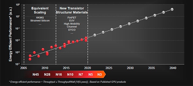
- Figure 11. History and projection of energy-efficient performance (throughput × throughput/Watt) of GPUs
- Note: Names such as N45 indicate scaling technology nodes (nm) at TSM.
Source: TSMC
[References]
- 1.
- ”Goodbye Moore’s Law” Nikkei Electronics (April 2015, pp.29-43)
- 2.
- Takeshi Hattori: “Moore’s Law survives, Transistor count still maintains a growth rate that doubles every two years.” Mynavi News TECH+ (March 24, 2020)
https://news.mynavi.jp/article/20200324-1001886/
- 3.
- Susumu Furuike of Sanyo Electric, “Scaling beyond 28 nm is meaningless” Nikkei xTECH news article (May 19, 2011)
He said this when he was formerly Vice President in charge of semiconductors at Panasonic. Note that Panasonic Corp. sold its entire semiconductor business, including three plants in Hokuriku, to a Taiwanese company in 2020, withdrawing from the semiconductor business.
https://xtech.nikkei.com/dm/article/NEWS/20110519/191938/
- 4.
- Takeshi Hattori: “Moore’s Law will survive beyond 1 nm. Imec and ASML collaborate to develop next-generation alignment technology.” Mynavi News TECH+ (November 27, 2020)
https://news.mynavi.jp/article/20201127-1531857/
- 5.
- Takeshi Hattori: “Imec announces validation results of micro FETs that use 2-nm forksheet devices and 2D materials.” Mynavi News TECH+ (December 16, 2020)
https://news.mynavi.jp/article/20191216-940012/
- 6.
- Takeshi Hattori: “Moore’s Law celebrates its 50th anniversary – When planar scaling reaches its limit, shift to 3D stacking.” Telescope Magazine (March 31, 2015)
https://www.tel.co.jp/museum/magazine/material/150327_report04_02/03.html
- 7.
- Takeshi Hattori: “Current status and future outlook of 3D IC technology discussed by TSMC chairman - ISSCC 2021” Mynavi News TECH+ (February 25, 2021)
https://news.mynavi.jp/article/20210225-1752851/
[Note]
- *1
- “The experts look ahead,” 35th-anniversary issue of Electronics magazine (launched on April 19, 1965)
- *2 Planar structure:
- Structure in which transistor surfaces are flat.
- *3 FinFET structure:
- Structure in which transistors gradually rise up on the substrate. Called “TriGate” by Intel.
- *4 α-nm:
- Equivalent to the 10-nm class fourth generation, coming after 1x-nm, 1y-nm, and 1z-nm. Estimated to be smaller than 15 nm, but companies have not published specific numbers.
- *5
- Intel’s 7-nm process, and TSMC’s and Samsung’s 5-nm processes, which are considered to be equivalent in performance.
- *6
- Indicates 1/2 length (half pitch) of the word line wiring pitch.
- *7
- Silicon chip consisting of only multi-layer wiring.
- *8 InFO:
- Stands for Integrated Fan-Out, which is TSMC’s unique way of naming a packaging method generally referred to as Fan-Out Wafer-Level Packaging (FOWLP).
- *9 CoWoS:
- Stands for Chip-on-Wafer-on-Substrate (wafer on a resin substrate and chips on that wafer).
- *10
- Method that stacks chips in the vertical direction.
- *11
- Method that stacks wafers in the vertical direction.
- *12
- Indicates utilization of a wired logic FPGA as a computation device, neuro computers, quantum computers, etc.
Writer
Takeshi Hattori
Takeshi Hattori worked at Sony Corporation for more than 30 years, working in a broad range of responsibilities, including semiconductor basic research at the Central Research Laboratories, and everything from device/process development to mass production yield improvement in the Semiconductor Business Division. During these years, he was involved in management and research planning work at the company headquarters, studied at Stanford University Graduate School, and was also a visiting researcher at the university’s Integrated Circuits Laboratory. Research fellow. Since 2007, Hattori has been an independent technology/management consultant and international technology journalist. He periodically publishes articles on the semiconductor industry and technology trends in Mynavi News TECH+ website, Nikkei xTECH website, the Semiconportal website, and Mainichi Shimbun Publishing's Weekly Economist magazine. PhD. Fellow/Lifetime honorary member of the Electrochemical Society (ECS). Author of several books including “Technology for Cleaning Silicon Wafer Surfaces,” in both a Japanese (Realize Corporation) and English version (Springer), “Supercritical Fluids for Semiconductors MEMS (Corona Publishing Co., Ltd.),” “Megatrend in Semiconductors 2014-2023 (Nikkei BP) (both coauthored with others).”


