


- Semiconductor Technology Now
Semiconductor Technology Now
Report Series
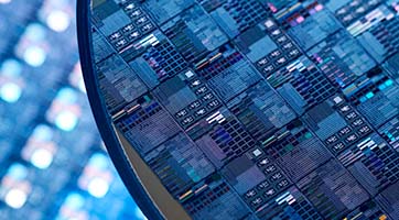
Steppers are key to full-scale 450 mm wafer processing
The main bottleneck for full-scale 450 mm wafer processing is lithography. The most promising system is an EUV stepper being developed by Dutch firm ASML, which uses the extreme ultraviolet wavelength of 13.5 nm. But the company is having trouble increasing the equipment's light source output and raising its throughput to the level of conventional steppers. ASML's rival Nikon shipped a prototype 450 mm ArF immersion stepper in April 2015, and has announced the plan to ship a production model in 2017 (or at a later date requested by customers). Nikon is expected to set the pace of transition to 450 mm wafers across the world for at least a few years. However, the methodology adopted by Nikon suffers from relatively low resolution as well as high production cost due to the complex multi-patterning process required for achieving nanoscale fabrication. In contrast, the EUV processing has higher resolution and requires only one exposure per process-advantages that are inducing many customers to wait for further refinement of this technology.
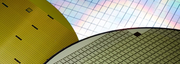
When will the transition to 450 mm technology begin?
Intel's initial plan announced in 2012 envisioned 450 mm prototyping to start in 2015-2016 and volume production in 2018. However, Intel faced an unexpectedly prolonged yield problem at its 300 mm lines for 14 nm microprocessors, as described in Part 1. Unless this problem is solved, the move to 450 mm lines could never take place. Moreover, Intel had announced entry into foundry services foreseeing a long-term decline in its staple PC microprocessor business, but the move stirred up heated competition among the 14 nm foundries and is distracting Intel from the 450 mm business, at least for the time being. To make matters worse, the prospect of 450 mm EUV steppers is still not very encouraging.
Intel concedes that its initial plan has been pushed back a few times already (and is practically shelved), but Intel president Brian M. Krzanich stated in October 2013 that the company was determined to start full-scale 450 mm production in the latter half of the 2010s, implying that Intel's official position hasn't changed all that much. If, however, the competition in foundry services among Intel, TSMC, and Samsung were to intensify in the 10 nm node, the shift to 450 mm production may be further delayed, especially as the yield improvement technology may take some time to develop.
In addition, construction of 450 mm plants will require even larger amounts of investment than with 300 mm plants, which means only a handful of semiconductor manufacturers in the world can afford to build them. To ensure the continued growth of the semiconductor industry as a whole, we need to assess the potential impact of the 450 mm technology from more diverse viewpoints, including those of the market and the economy.
The contents of the article is at the time of announcement.
Writer
Takeshi Hattori
Hattori worked at Sony Corp. for over 30 years, doing basic research on semiconductors at the company's Central Laboratory and taking a wide range of responsibilities at the Semiconductor Business Group, including device process development and improvement of production yields. During his tenure at Sony, Hattori also served as a member of the headquarters management/research planning team, studied at Stanford University (graduate school) to receive an engineering doctorate, and became a visiting scholar at the university's integration circuit laboratory. Hattori left Sony in 2007 to become a technology/management consultant and international technology journalist. He is a Fellow and board member of the Electrochemical Society (ECS), and a visiting professor of engineering at Hanyang University in Korea. Among the books he co-authored are Ultraclean Surface Processing of Silicon Wafers (Japanese version published by Realize Corporation, English version by Springer International Publishing), Supercritical Fluid Technology in MEMS and Semiconductor Processing (in Japanese, Corona Publishing Co., Ltd.), and Megatrend Semiconductors 2014-2023 (in Japanese, Nikkei BP).
Contents
Cross Talk
Visiting Laboratories
Expert Interview
Topics
Report Series

- Motorization, Act II – The Age of Automated Driving

- How Society Will Change in the Digital Age
- Part 1
- What is Digitalization?

- Sports Technology Protecting Athletes and Providing Fairer Refereeing