


- Semiconductor Technology Now
Semiconductor Technology Now
Report Series
Japan leads the world in silicon wafer manufacturing
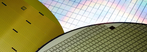
Here's how silicon wafers are made: first, multicrystalline silicon of high purity is crushed into powder and put into a crucible made of quartz, and then heated until the powder melts. Next, a small stick of seed crystal hung from the end of a wire is dipped into liquid silicon. As the stick is rotated and slowly pulled up, an ingot of monocrystalline silicon is formed that has the same atomic arrangement as the seed crystal (Figure 3, top). The cylindrical ingot is then sliced into thin circular wafers, which are polished, etched, and cleaned multiple times until their surface is as shiny as a mirror (Figure 3, bottom).
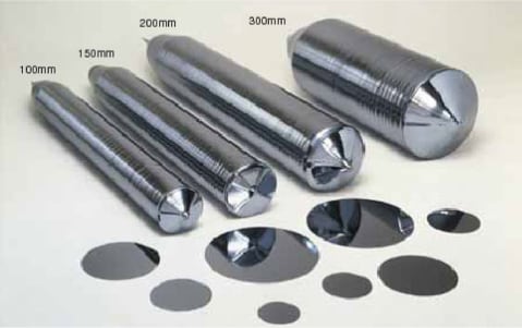 |
Pulling up a silicon ingot without crystalline defects requires subtle and difficult control of temperature and pulling speed. The first ingots were only 0.75 inch (20 mm) in diameter, but half a century of trials and errors later, it finally became possible to manufacture 300 mm (12-inch) ingots. That means the wafer diameter increased 16 times and the wafer area by 250 times in the same period. Global shipment of silicon wafers in 2014 increased 11.4% over the previous year, reaching a record high of 9.37 billion square inches (6.045 million square meters) in volume, or $7.6 billion in value.
The top supplier of silicon wafers in the world is Shin-Etsu Handotai Co., Ltd. (SEH), a wholly-owned subsidiary of Shin-Etsu Chemical Co., Ltd. The second largest supplier is also a Japanese company, SUMCO, although the name is probably unfamiliar to those outside the field. The company was formed in 2002 as Sumitomo Mitsubishi Silicon Corp. in a merger between Mitsubishi Materials Silicon Corp. and the Sitix Division of Sumitomo Metal Industries, Ltd. The company changed its name to SUMCO in 2005, and acquired Komatsu Electronic Metals Co., Ltd. the following year. One might say the three rivals of Shin-Etsu joined forces as SUMCO. These top two suppliers control more than 60% of the silicon wafer market worldwide, proving the excellence of Japanese firms in producing defect-free silicon wafers.
A shift to 450 mm wafers could cut costs by 30%
Each new scaling node of semiconductor devices requires new materials and new technologies such as higher resolution lithography, which causes production cost to soar. That is why efforts to control cost by making wafer diameters larger have been ongoing for over a half century (Figure 4).
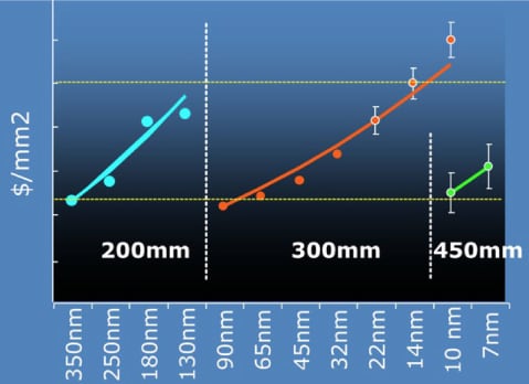 |
Based on past experience, the industry is seeking to absorb the rising production cost of advanced devices by increasing the wafer diameter from 300 mm to 450 mm or by 50% (thereby enlarging the wafer area by 2.25 times).
According to an estimate by SEMATECH (a consortium of semiconductor manufacturing technology developers), production cost per chip will be down by 30% if 450 mm wafers were adopted to replace 300 mm wafers, provided that the price of 450 mm wafers is no more than 5.5 times that of 300 mm wafers and the purchase price of the 450 mm manufacturing equipment (including their cost for utilities, consumables, and maintenance) does not exceed 130% that of 300 mm equipment (Table 1). Encouraged by this prospect, more and more semiconductor manufacturers around the world are considering a shift to 450 mm wafers.
| Cost component | Percentage in total cost | Increase in cost (times) | Increase in production (times) | Effect on expenditure |
|---|---|---|---|---|
| Manufacturing equipment | 50% | 1.3 | 2.3 | −45% |
| Utilities and maintenance | 19% | 1.3 | 2.3 | −45% |
| Silicon substrate | 7% | 5.5 | 2.3 | +135% |
| Materials (chemicals, gases, consumables) | 24% | 1.3 | 2.3 | −45% |
| Total (wafer cost) | 100% | 1.3 | 2.3 | −32% |
Contents
Cross Talk
Visiting Laboratories
Expert Interview
Topics
Report Series

- Motorization, Act II – The Age of Automated Driving

- How Society Will Change in the Digital Age
- Part 1
- What is Digitalization?

- Sports Technology Protecting Athletes and Providing Fairer Refereeing