


- Semiconductor Technology Now
Semiconductor Technology Now
Report Series
Five leading firms form a U.S.-based consortium to pursue transition to 450 mm wafers
Intel knew from past experience that an early shift to 450 mm wafers was imperative in avoiding the steep rise in chip manufacturing cost associated with advanced scaling. Accordingly, the company approached Samsung of Korea and TSMC of Taiwan and announced a joint development plan for 450 mm technology in May 2008. The plan failed to gain support of the clients (i.e., semiconductor manufacturers), however, because they were still in the process of recovering their investment in 300 mm equipment. Consequently, the plan to start prototyping in 2012 had to be abandoned.
Then on September 26, 2011, New York State Governor Andrew M. Cuomo made a surprise announcement that five leading semiconductor manufacturers (Intel, TSMC, Samsung, GlobalFoundries, and IBM) were initiating two major projects in Albany, N.Y.; one for creating the next-generation computer chip technology and another for introducing the 450 mm wafer. The statement quickly brightened the prospect for the 450 mm wafer technology.
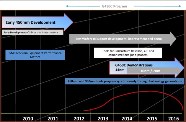
In 2012, the five companies mentioned above participated in the Global 450mm Consortium (G450C) led by New York State and the Colleges of Nanoscale Science and Engineering (CNSE) of the New York State University at Albany. The consortium's stated goal was to evaluate 450 mm equipment, assess 14 nm node process technologies, and establish a practical manufacturing environment so the member firms can build a 450 mm pilot line by 2015-2016. The goal was subsequently revised, and now includes assessing 10/7 nm node equipment and technologies by the end of 2016 (Figure 5).
 |
According to the G450C, early assessments of 450 mm equipment were quite favorable and no major technological obstacle was foreseen in the transition from 300 mm to 450 mm, except for the 450 mm stepper which is yet to be developed and tested (to be discussed later).
European semiconductor equipment industry supports migration to 450 mm wafers
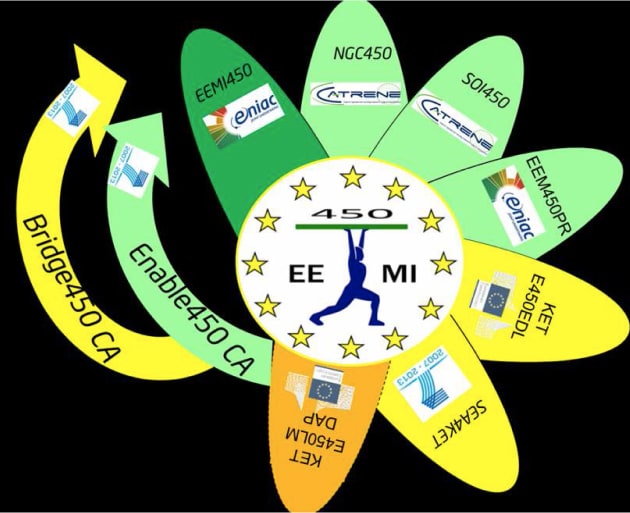
In Europe, semiconductor equipment and materials manufacturers are promoting the migration to 450 mm wafers, establishing the European 450mm Equipment and Materials Initiative (EEMI450) in 2009. With financial support from the European Commission, an EEMI450 project for developing 450 mm equipment and materials was implemented from 2010 through 2012. After the project ended, the EEMI450 has remained active as a 450 mm platform for Europe, with the membership increasing to 58 companies in 10 countries. The initiative has spawned a number of public-sector supported projects for 450 mm technology promotion that are being implemented in parallel (Figure 6). The entire initiative is backed by such projects as the Enable450 project for linking and disseminating 450 mm technology-related information, as well as the Bridge450 project that aims to cultivate potential demand for 450 mm equipment in Asia and elsewhere and to lure 450 mm fabs to Europe.
 |
Imec, an independent research institute of advanced semiconductors in Belgium, is currently building a cleanroom for R&D in 450 mm technologies, with financial assistance from the Flemish Government.
In Israel, an industry-government-academia partnership on 450 mm metrology called Metro450 has been inaugurated. The project has been promoting global cooperation between the G540C and the EEMI regarding the evaluation of 450 mm equipment.
Contents
Cross Talk
Visiting Laboratories
Expert Interview
Topics
Report Series

- Motorization, Act II – The Age of Automated Driving

- How Society Will Change in the Digital Age
- Part 1
- What is Digitalization?

- Sports Technology Protecting Athletes and Providing Fairer Refereeing