- Japanese
- English
JavaScript is disabled.
Please enable JavaScript to watch this content.
Buliding nanoscale structures with precision
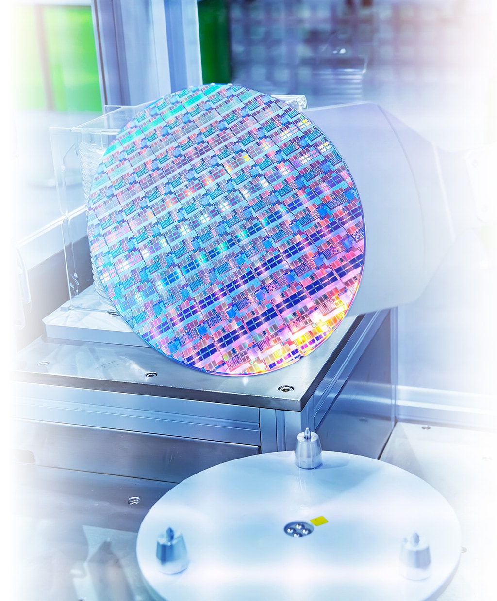
The manufacture of semiconductors is a highly interdisciplinary process involving physics, chemistry, electricity, electronics, metallurgy and more. Today, it has become so advanced that the purity of silicon used for semiconductors can be as high as 99.999999999% (eleven nines).
Let’s take a look at the latest nanotechnology-enabled How Semiconductors are made step by step, together with the equipment used.
