- Japanese
- English
JavaScript is disabled.
Please enable JavaScript to watch this content.


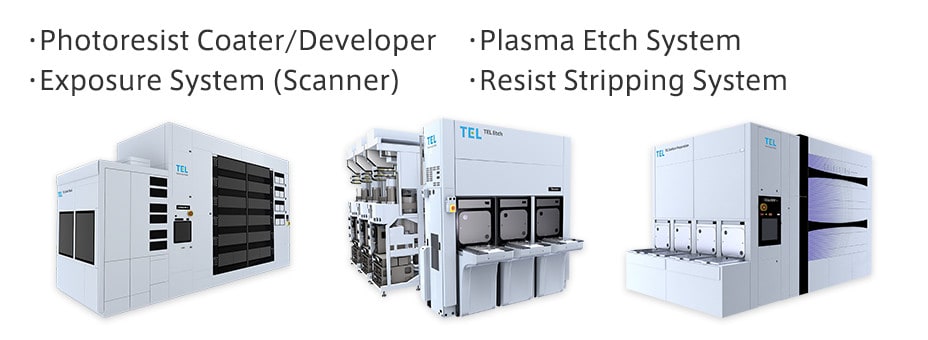
The patterning process is implemented on a dielectric film to make contact holes.
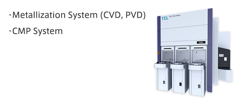
The voids are filled with metal using the CVD process. Excess metal film is polished off.
An intermetal dielectric film (such as low-k film) is deposited on the surface. The patterning process is then implemented to cut trenches where wires are to be laid.
The trenches are filled with a metal layer, and the surplus metal is polished off. The cycle of intermetal layer deposition, trench filling with metal, and planarization is repeated until the necessary numbers of wiring layers are formed.