- Japanese
- English
JavaScript is disabled.
Please enable JavaScript to watch this content.


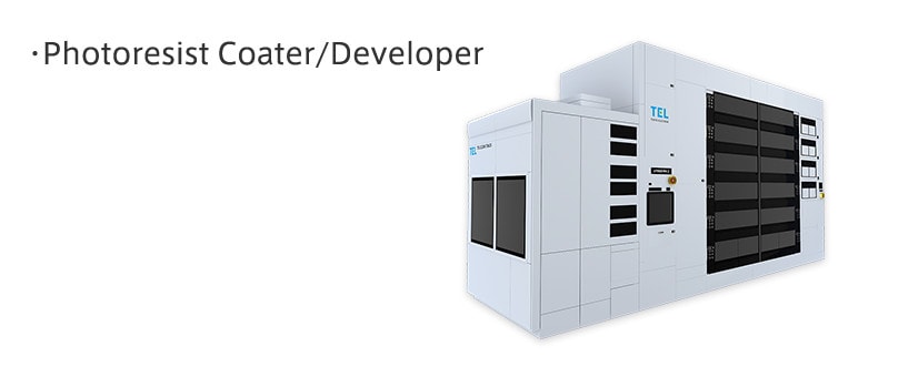
The coater spins a wafer at high speed and uniformly applies a UV-sensitive photoresist on its surface.
The stepper aligns the circuit pattern drawn on a glass mask over a wafer coated with photoresist, and then irradiates ultraviolet (UV) light to transfer the pattern onto the photoresist.
The developer applies a liquid developing agent uniformly over the wafer to fix the transferred image. Exposed area becomes soluble in developer in the case of positive-type photoresist, and unexposed area becomes soluble in the case of negative-type photoresist. That is how etch mask pattern is generated in photolithography.
Plasma etchers etches films of unmasked area by photoresist.

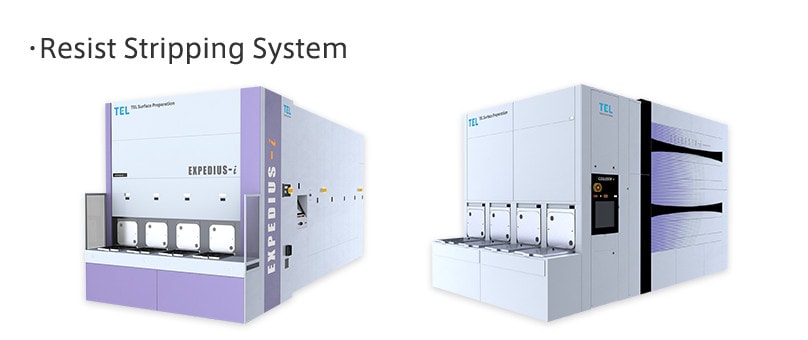
After etching, photoresist is removed by ashing.
Wet cleaning frequently follows ashing in order to remove residues.