JavaScript is disabled.
Please enable JavaScript to watch this content.
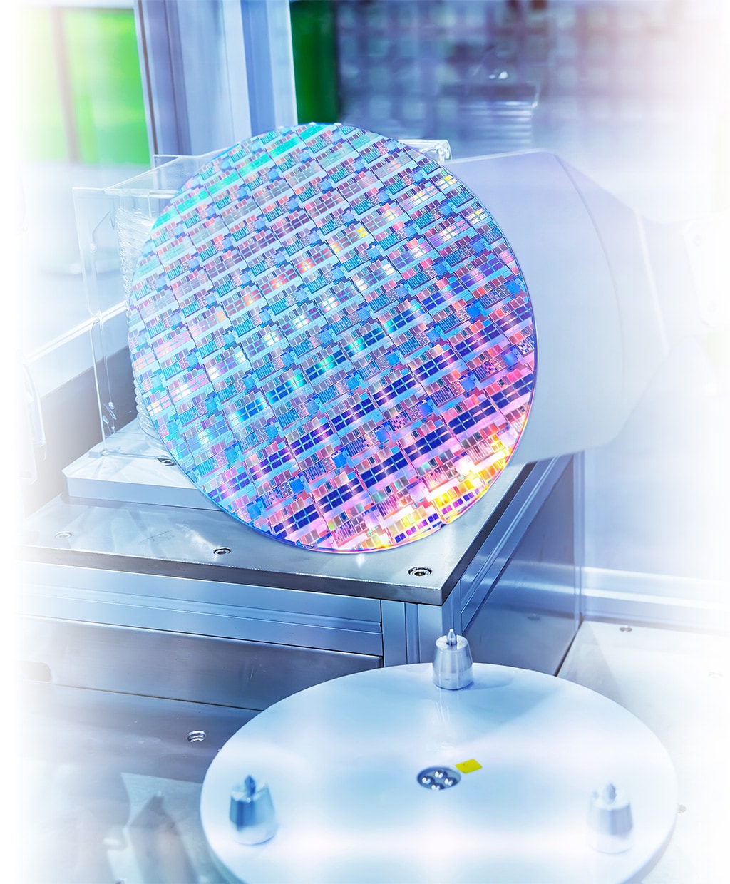
How Semiconductor is made

10
Gate Formation

Gate Dielectric Film Formation / Gate Electrode Formation

RESTART

A gate dielectric film (oxide film) is deposited by thermal oxidation, followed by surface nitriding treatment. A gate electrode layer (polysilicon film) is then deposited by the CVD process.

Semiconductor equipment

Dielectric Film Deposition System, Metal Deposition System (CVD, PVD)
11
Gate Formation

Patterning

RESTART

The patterning process is implemented on the gate electrode layer to form the source and drain region.

Semiconductor equipment

Photoresist Coater/Developer, Exposure System (Scanner)
12
Gate Formation

Ion Implantation / Annealing

RESTART

The elements extracted by the ion implantation process (boron, arsenic, etc.) are doped into the source and drain region. The area covered by the residual oxide film is not doped. The doped impurities are spread uniformly in the trenches by means of high temperature anneal.

Semiconductor equipment

Ion Implant System, Exposure System (Scanner)
13
Gate Formation

Intermetal Dielectric Film Formation / Planarization

RESTART

An oxide film is deposited through the CVD process to form an intermetal dielectric film, and the surface is polished and planarized.

Semiconductor equipment

Low-pressure (LP) CVD System, CMP System
PREV NEXT