


- Semiconductor Technology Now
Topics
Product
The race among 16/14 nm semiconductor foundries to intensify this year
As the ITRS 2013 (Table 1) indicates, mass production of 14/16 nm logic devices was supposed to start before the end of 2013. However, Intel has had trouble improving the production yield of its 14 nm MPUs for a long time, and it was in the latter half of 2014 that the company finally shipped a small amount of 14 nm tablet MPUs from its prototyping line in Oregon. Mass production of 14 nm MPUs for PCs is now pushed back to 2015. That means switching to the 14 nm logic technology node will take more than three years instead of customary two. Intel announced in fall 2013 that it would begin the foundry service business starting with 14 nm products. As the problem with production yield has not been completely solved, though, the start of Intel’s foundry service is expected to be delayed until the production of 14 nm MPUs for PCs gets on track in the latter half of 2015 or later.
 |
Competition intensifies among leading-edge semiconductor manufacturers
The latest battlefront of the semiconductor business is in the 14 nm technology, where leading manufacturers such as Intel, Samsung, and TSMC play the key part. The intensity of their competition may be glimpsed from the following episodes.
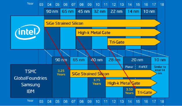
At the time Intel announced its entry into the foundry service business, the company claimed it had consistently adopted new technologies three or more years ahead of its rivals (Fig. 4). Intel’s not-so-subtle disparagement of its rivals seems to reflect how badly the company had been suffering from sluggish sales in the mobile computing sector.
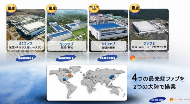
Meanwhile, Samsung skipped the 20 nm node and pressed on with the development of the 14 nm FinFET process, completing it in the first half of 2014 and declaring production would start in fall 2014 before Intel’s foundry service was to begin. Reportedly, the company has already won large orders from multiple customers, or is likely to secure them. Rumors have it that Samsung’s S2 fab in Austin, Texas is already prototyping the A9 processor for Apple’s next-generation iPhones and iPads (scheduled for release in fall 2015). Samsung has also licensed its 14 nm process to U.S.-based GlobalFoundries (GF), and announced the start of 14 nm device production services jointly with GF in April 2014 (Fig. 4). GF is now getting ready to go into production.
 |
Not to be outdone by Intel that was new to the foundry business, Taiwan’s TSMC performed a tour de force of developing the 20 nm and 16 nm processes in parallel. As a result, the company won exclusive orders for 20 nm devices in 2014 from major global clients including Apple, and embarked on risk production of 16 nm devices in fall 2014.
The three-way foundry battle among Intel, TSMC, and Samsung (with its technology licensee GlobalFoundries) is about to begin in earnest. As the technology node shifts from 14 nm to 10 nm, the difficulty of scaling would multiply, and many things certainly won’t go as predicted in the ITRS roadmap. In fact, the predictions given in the ITRS have become increasingly unreliable lately. Perhaps it would be more prudent to think of them as industry goals.
While conventional ICs have only scratched the surface of a silicon substrate, emerging new technologies make use of multiple silicon layers to form 3D structures of much higher circuit density. In the next article, I will discuss the future direction of 3D technologies and how far the chip scaling would go.
The contents of the article is at the time of announcement.
Writer
Takeshi Hattori
Hattori worked at Sony Corp. for over 30 years, doing basic research on semiconductors at the company’s Central Laboratory and taking a wide range of responsibilities at the Semiconductor Business Group, including device process development and improvement of production yields. During his tenure at Sony, Hattori also served as a member of the headquarters management/research planning team, studied at Stanford University (graduate school) to receive an engineering doctorate, and became a visiting scholar at the university’s integration circuit laboratory. Hattori left Sony in 2007 to become a technology/management consultant and international technology journalist. He is a Fellow and board member of the Electrochemical Society (ECS), and a visiting professor of engineering at Hanyang University in Korea. Among the books he co-authored are Ultraclean Surface Processing of Silicon Wafers (Japanese version published by Realize Corporation, English version by Springer International Publishing), Supercritical Fluid Technology in MEMS and Semiconductor Processing (in Japanese, Corona Publishing Co., Ltd.), and Megatrend Semiconductors 2014-2023 (in Japanese, Nikkei BP).
Contents
Cross Talk
Visiting Laboratories
Expert Interview
Topics
Report Series

- Motorization, Act II – The Age of Automated Driving

- How Society Will Change in the Digital Age
- Part 1
- What is Digitalization?

- Sports Technology Protecting Athletes and Providing Fairer Refereeing