


- Semiconductor Technology Now
Topics
Product
Semiconductor scaling indicator loses touch with physical dimensions
The pace of gate length reduction has been slowing in recent years, however, due to what is known as the short-channel effect. This phenomenon becomes more pronounced as gate length gets shorter, adversely affecting the electrical property of the device and causing malfunctions if there is the slightest variance in gate length. As the annual rate of gate length reduction has decreased, it became inconvenient to use gate length as the indicator of semiconductor scaling. So the industry is now simply multiplying the numerical value of the previous technology node by 0.7 for each new technology node, which comes every two or three years with the introduction of new materials and structures.
During the 1980s and 1990s when DRAM was the leading technology product, each new technology node reduced the minimum linewidth to 0.7 times what it was in the previous node. This convention has been retained in the recent labeling of technology nodes, although the numerical values no longer have any bearing on physical dimensions. That is why the second line of the leftmost column in Table 1 reads Logic Industry “Node Name” Label instead of Technology Node. Because the figures are just labels devoid of physical meaning, they are presented as absolute numbers in this table, but few other publications follow this practice, and they attach the conventional unit (nm) instead. As Table 1 demonstrates, the value in the node name does not correspond to any of the dimensions listed underneath it. The most advanced device node currently being ramped up for mass production is called 16 nm by TSMC and 14 nm by Intel and Samsung, but we cannot ascertain their actual levels of scaling and performance until the products are released.
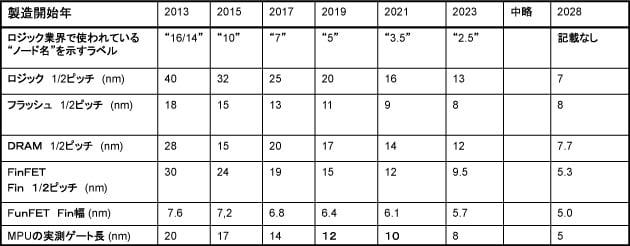 |
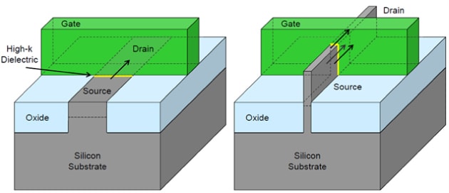
Arrival of a 3D transistor structure
A new transistor structure has emerged that can reduce performance variance by diminishing the short-channel effect. The technology uses a gate to enclose the channel on multiple sides and prevent minuscule leakage of carriers (electrons and holes). The adoption of a 3D structure also has the advantage of making transistors even smaller. Intel was the first in the world to announce this 3D structure, enclosing the 22 nm node MOS transistor channel’s three sides with a gate. Intel calls this structure Tri-gate (Fig. 2, right), although it is popularly referred to as FinFET, from the shape of the channel that resembles a fin. Intel’s rivals will be adopting this structure several years behind Intel, starting in the 16/14 nm node. As is evident from Table 1, the minimum processing dimension in this structure is the FinFET width (the width of the gray fin that runs through the green gate at right angles in Fig. 2, right), which is about 7 nm and not 16 or 14 nm.
 |
Contents
Cross Talk
Visiting Laboratories
Expert Interview
Topics
Report Series

- Motorization, Act II – The Age of Automated Driving

- How Society Will Change in the Digital Age
- Part 1
- What is Digitalization?

- Sports Technology Protecting Athletes and Providing Fairer Refereeing