


- Semiconductor Technology Now
Expert Interview
Telescope Magazine: What’s the next level of innovation after the first CMOS annealing chip?
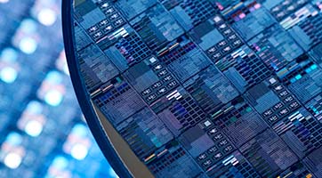
Masanao Yamaoka: This is the first-generation CMOS annealing LSI chip. For the prototyping of second- and third-generation chips, we used a field programmable gate arrays or FPGA*6 (Figure 5). The advantage of using an FPGA is that the chip can easily be reprogrammed to adopt new and even more efficient algorithms as they come.
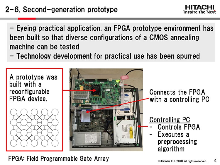 |
The first-generation CMOS annealing machine used an application-specific integrated circuit (ASIC)*7, which meant the configuration of the Ising model was fixed. However, there was room for improving the Ising model that we initially used, by varying the state and the strength of spin-spin coupling. Since ASIC precluded reprogramming, we decided that an FPGA would be preferable for the second-generation prototype. Now that we learned how effective the first chip was, we went on to build the second-generation machine with an FPGA board, so that new algorithms and parameters could be easily introduced.
Telescope Magazine: And the third-generation FPGA model? How is it different?
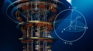
Masanao Yamaoka: The third-generation model (Figure 6) changed the annealing method to SQA, or simulated quantum annealing*8. The concept for this method emerged about 10 years ago, and Google announced at an academic conference in 2016 that quantum effects could be simulated by software. That inspired us to introduce this software into our hardware and improve the accuracy of prediction. We used an FPGA for its implementation.
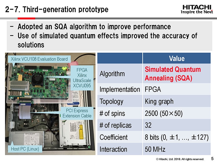 |
To put it simply, we build a number of replicas of an Ising model and then perform separate calculations, eventually letting the results converge into a solution. The process simulates the principle of quantum superposition. While in reality an infinite number of quantum effects can be superposed, our system is capable of superposing up to 32 or 64 layers of effects. This superposition is the key to improving the accuracy of solutions.
In fact, a simulation of a 32-layer superposition was found to be capable of solving an optimization problem 15 to 40 times faster than with conventional simulated annealing method.
Telescope Magazine: How are the layers represented in CMOS annealing?
Masanao Yamaoka: The layers are represented as parts of SRAM for the CMOS chip. We can make a somewhat larger SRAM and assign layer 1 to memory block 1 and layer 2 to memory block 2, and so on. Connections are the same for all layers, and only the spin values are different for each layer, so there is no need to make inordinately large SRAMs.
Telescope Magazine: Are you facing any practical issues with this technology?
Masanao Yamaoka: The hardware architecture has already been established, so we are now developing the software that can put the hardware to practical use. Let me give you an example. The spins in an Ising model are intricately interconnected to form a peculiar landscape, whereas an annealing machine has a very regular structure. So, we are developing a converter program to reproduce the complex interconnections on a regularly structured machine. This would keep the hardware simple, allowing the machine to solve the problem faster. The software development is thus critical to the practical application of this technology.
Telescope Magazine: Are there any problems with the CMOS annealing method or with quantum effects?
Masanao Yamaoka: Because CMOS annealing and quantum technologies as a whole represents a new field, figuring out the areas of application and developing suitable software programs can be challenging. The importance of software development is paramount, whether it is CMOS annealing or quantum annealing. Besides us, many other researchers in this field throughout the world are also working assiduously on software development.
One of the problems with CMOS annealing is that its solutions are less accurate than those obtained by a quantum computer. Given the same timeframe to calculate a problem, a CMOS annealing machine is no match for a quantum computer, and if a solution has to be calculated to a given degree of accuracy, the CMOS machine would certainly take longer. One way to address this issue will be to enhance the algorithm, as in simulated quantum annealing.
Another challenge is to assess the level of the solution accuracy required in real-world applications from an engineering viewpoint. This is critical because aiming for unnecessarily high accuracy is pointless and wasteful.
Prime factorization, for example, is a type of combinatorial optimization problem that is used for decryption. Since accuracy is the top priority in decryption, a quantum computer would be required for this type of operation. It is generally believed that if you have the ability to decompose any number to a group of prime factors, you can decrypt any encrypted message.
In contrast, some other applications only require an approximation to optimal solution. For example, optimization of your financial portfolio involves diverse parameters that change with the times, and you need a quick answer, so a near optimal solution would have to suffice. CMOS annealing is well-suited for this type of problem.
Telescope Magazine: That reminds me of voice and text recognition technologies used in AI speakers and so on. These technologies may not be perfectly accurate but are nearly optimal, which is important in practice.
Masanao Yamaoka: Exactly. These technologies perform certain levels of recognition, and then the results are approximated into words that are more or less in context. So, strict accuracy of recognition is not required.
Along with accuracy, the scale of operations needs to be taken into account. Weighing the scale of a problem and the given timeframe to solve it, you need to determine which computing method is more advantageous.
I think quantum computers are also making strides in terms of efficiency. CMOS annealing machines and quantum computers are not mutually exclusive. In fact, they can complement each other if suitable applications are found based on their respective strengths.
Footnotes
- *6
- FPGA (field programmable gate array): A digital logic circuit that is user-configurable by programming.
- *7
- ASIC (application-specific integrated circuit): An IC customized for a particular use and cannot be reconfigured.
- *8
- SQA (simulated quantum annealing): A computational simulation of quantum annealing, which uses a quantum-mechanical superposition of all candidate solutions and applies a time-dependent Schrödinger equation to find an optimal solution.
Contents
Cross Talk
Visiting Laboratories
Expert Interview
Topics
Report Series
- Motorization, Act II – The Age of Automated Driving

- How Society Will Change in the Digital Age
- Part 1
- What is Digitalization?

- Sports Technology Protecting Athletes and Providing Fairer Refereeing