
- Semiconductor Technology Now
Expert Interview
Telescope Magazine: How do you go about solving a combinatorial optimization problem?
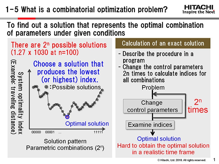
Masanao Yamaoka: If a combinatorial optimization problem has an n number of parameters, then there are 2 to the nth power (2n) possible solutions. To determine the optimal parametric combination for a traveling salesman problem, a graph may be drawn as in Figure 2, by plotting the system optimality index (traveling distance in this case) on the y-axis and the combination patterns on the x-axis. The combination of parameters that produces the least distance is the optimal solution. If there are 100 parameters, the number of possible combinations is 2100, which is a very large number.
 |
To solve this type of problem, D-Wave Systems of Canada has developed a quantum annealing machine. Because it uses superconducting devices to control the quantum states of matter, the machine has to be refrigerated to temperatures close to absolute zero. Although the machine is reputed to be the fastest in the world, it has practical issues including those associated with refrigeration. Also, the superconducting devices still need to overcome scalability challenges, which probably won’t be achieved anytime soon.
That is why we at Hitachi have proposed the CMOS annealing machine. It involves using conventional CMOS device technology to digitally simulate quantum annealing. Its processing speed may be slower than that of a quantum annealing machine, but it does not need refrigeration and is scalable, which are distinct advantages. As it’s easy to handle and applicable to large-scale calculations, it will be particularly suitable for scalable applications.
Telescope Magazine: How does an annealing machine work?
Masanao Yamaoka: The operating principle of an annealing machine derives from the Ising model, named after German physicist Ernst Ising. Consider, for example, a square-lattice of magnetic particles as in Figure 3. The direction of the spin magnetic moment of each particle is either upward (shown in red) or downward (blue). Depending on the spin distribution of magnetic particles on the lattice, the total energy of this Ising model changes, and the model stabilizes when the energy is the lowest, which is the optimal state. In an Ising model, the spin states are considered to continue shifting until they reach the point where the total energy is the lowest (see graph on the right in Figure 3).
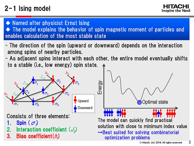 |
In a combinatorial optimization problem, the parameters are mapped to the Ising model to determine the point of lowest energy, and then the identified parameter set is put back to the optimization problem to obtain the solution. At Hitachi, we’ve been using CMOS devices instead of magnetic particles in constructing the Ising model. The upward and downward spins are substituted by 1 and 0 states of memory bits in SRAM*4. This is the approach we refer to as CMOS annealing.
Telescope Magazine: Why use CMOS?
Perhaps quantum computers would be a better choice if the goal is to achieve superior performance in the long run, but CMOS is more advantageous in addressing immediate needs. Another reason we chose CMOS was that it has many applications including mobile phones. Implementing the annealing technology on semiconductor chips makes sense because they are readily accessible, and the semiconductor industry has a proven record of reliability and experience.
Telescope Magazine: Specifically, how do you execute annealing on CMOS?
Masanao Yamaoka: We use a digital circuit to simulate the shift of energy to a lower state. In Figure 4, the top right lattice represents the state where the system’s energy is the highest, with all spin directions being the same. Then we change the spin states in steps so the energy level is reduced. To prevent any trapping at a local minimum point, the changes are occasionally randomized to introduce radically different spin value patterns. When the point of apparently lowest energy is reached, that is taken to be the practical solution*5.
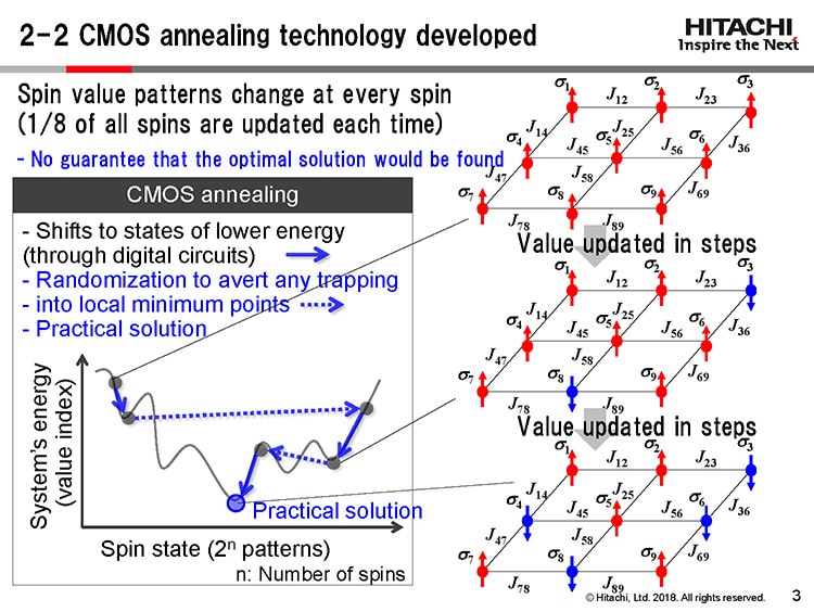 |
I used the term “practical solution” here, because the lowest value reached with this method may not be the lowest possible value. After all, the method does not exhaustively test all possible patterns but rather chooses sample patterns randomly. The solution is of practical use nevertheless, hence the term “practical solution.”
We’ve built a prototype CMOS chip capable of handling 20,480 spins, and measured the time it took to solve a combinatorial optimization problem, with the result that its energy efficiency was 1,800 times greater than that of a conventional CPU solving the same problem. With small scale problems, such as those involving only 8 spins, the difference was only four times or so. But the energy efficiency of the CMOS chip steadily grew with the scale of the problem, reaching 1,800 times of a conventional CPU at 20,480 spins.
Telescope Magazine: How do you define energy efficiency in this instance?
Masanao Yamaoka: It is defined as the amount of power consumed before the problem was solved to the given level of precision. The CPU used for comparison was an Intel Core i5, a representative CPU for personal computers, running the program at 1.87 GHz and 10 W/core. For the sake of comparison, the energy efficiency value of this CPU is set at 1.
Footnotes
- *4
- SRAM: An abbreviation for static random access memory. SRAM uses bistable flip-flop circuitry to store 0 or 1. SRAM is volatile and loses its data when the power is off, but the data are retained as long as the SRAM remains powered.
- *5
- Practical solution: A solution that suffices in practical use. It may not be the absolutely correct solution, but often it is close enough to be treated as such.


