


- Semiconductor Technology Now
Semiconductor Technology Now
Report Series
Part 3
From 20 mm to 450 mm: The Progress in Silicon Wafer Diameter Nodes
- April 30, 2015

In the last article, I described how the semiconductor industry has consistently reduced the manufacturing cost per transistor for over half a century by raising the integration level through device scaling. There are also many other factors that have contributed to this cost reduction, however. Examples include the efforts made at production sites, including the improvement in production yield (non-defect rate) and throughput (production volume per unit of time), as well as the industry trend for adopting ever larger silicon wafer diameters (Figure 1).
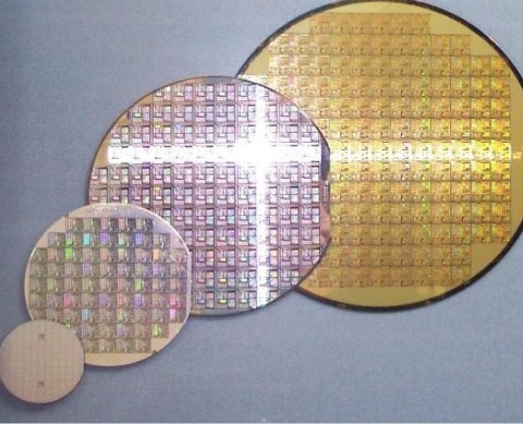
As the area of wafer surface increases, the number of semiconductor chips (dies) that can be obtained from a wafer also increases, reducing the production cost per chip. Part 3 of this series will focus on the historical industry trend of wafer diameter growth as an effective means to reduce semiconductor production cost, and attempt to foresee how soon the next-generation 450 mm wafer will become the mainstream.
 |
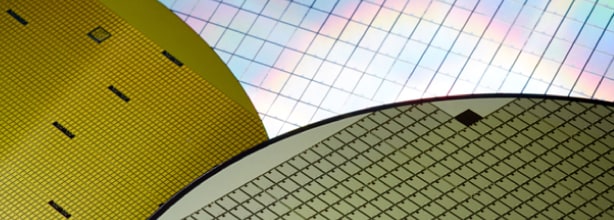
The history of semiconductors is the history of increasing wafer size
The history of semiconductors has paralleled the shrinking of circuit dimensions as well as the increase in wafer size (Figure 2). In the early 1960s, monocrystalline silicon wafer of 0.75 inch (about 20 mm) in diameter became available. Around the time Gordon Moore presented the so-called Moore's law in 1965 (see Part 2), 1.25-inch (30 mm) wafers that had been sparingly used for the manufacture of discreet transistors were replaced by 1.5-inch (40 mm) wafers, as demand surged in order to produce early integrated circuits (ICs).
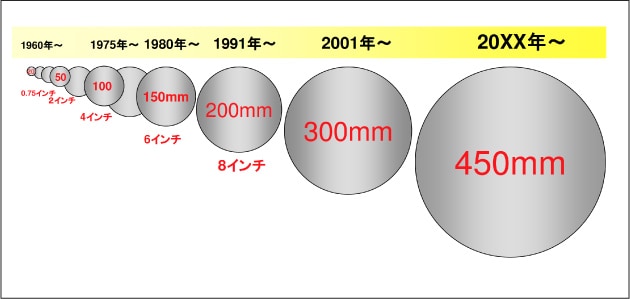 |
This was followed by 2-inch (50 mm) and 3-inch (75 mm) wafers, before 4-inch (100 mm) wafers emerged around 1975 to become the mainstream throughout the world. The trend continued as shown in Figure 2, with successive introduction of 5-inch (125 mm), 6-inch (150 mm), and 8-inch (200 mm) wafers. The 21st century has brought us to the 300 mm age, and that's where we are right now.
The latest semiconductor production lines today use 300 mm wafers for logic/memory chips and for analog devices. In contrast, production lines built in the 1980s and 1990s use 6- and 8-inch wafers, and there are some older production lines that still use 4-inch wafers.
Let me digress a little here to talk about the measurement of wafer diameters. Because the transistor and the process for growing silicon ingots were both invented in the U.S., the country's customary system of measurement (the international yard and pound that are now only used in the U.S.) had traditionally been employed across the world for measuring wafer diameters. Around the time when 8-inch wafers became dominant, however, Americans began to use metric measurements for wafer diameters. In a strange reversal of roles, more and more Americans came to refer to "200 mm wafers," while their Japanese counterparts often persisted with traditional "8-inch wafers." Since then, however, metric measurements have prevailed worldwide in this field, so now we are in the "300 mm" era.
Contents
Cross Talk
Visiting Laboratories
Expert Interview
Topics
Report Series

- Motorization, Act II – The Age of Automated Driving

- How Society Will Change in the Digital Age
- Part 1
- What is Digitalization?

- Sports Technology Protecting Athletes and Providing Fairer Refereeing