JavaScriptが無効になっています。
このWebサイトの全ての機能を利用するためにはJavaScriptを有効にする必要があります。


- Report Series
Let’s dig deep into complex supply chain of semiconductor industries!
- Text by Kenji Tsuda
- 2024.02.07
As with the iPhone, many companies engage in semiconductor supply chains. Companies from all over the world are participating. As semiconductor integrated circuits (ICs) become more integrated and more complex, any one company could not handle all process operations. Various companies, including some really surprising ones, contribute to the production of modern ICs. As one example of these companies, Ajinomoto, a very famous food company, is the largest supplier of advanced packaging substrates. Let me explain what kind of design tools, materials, and manufacturing equipment are necessary as well as what industries that supply those engage in the production of semiconductor chips.
What is an IC Chip?
An IC chip is a circuit in which transistors are integrated.
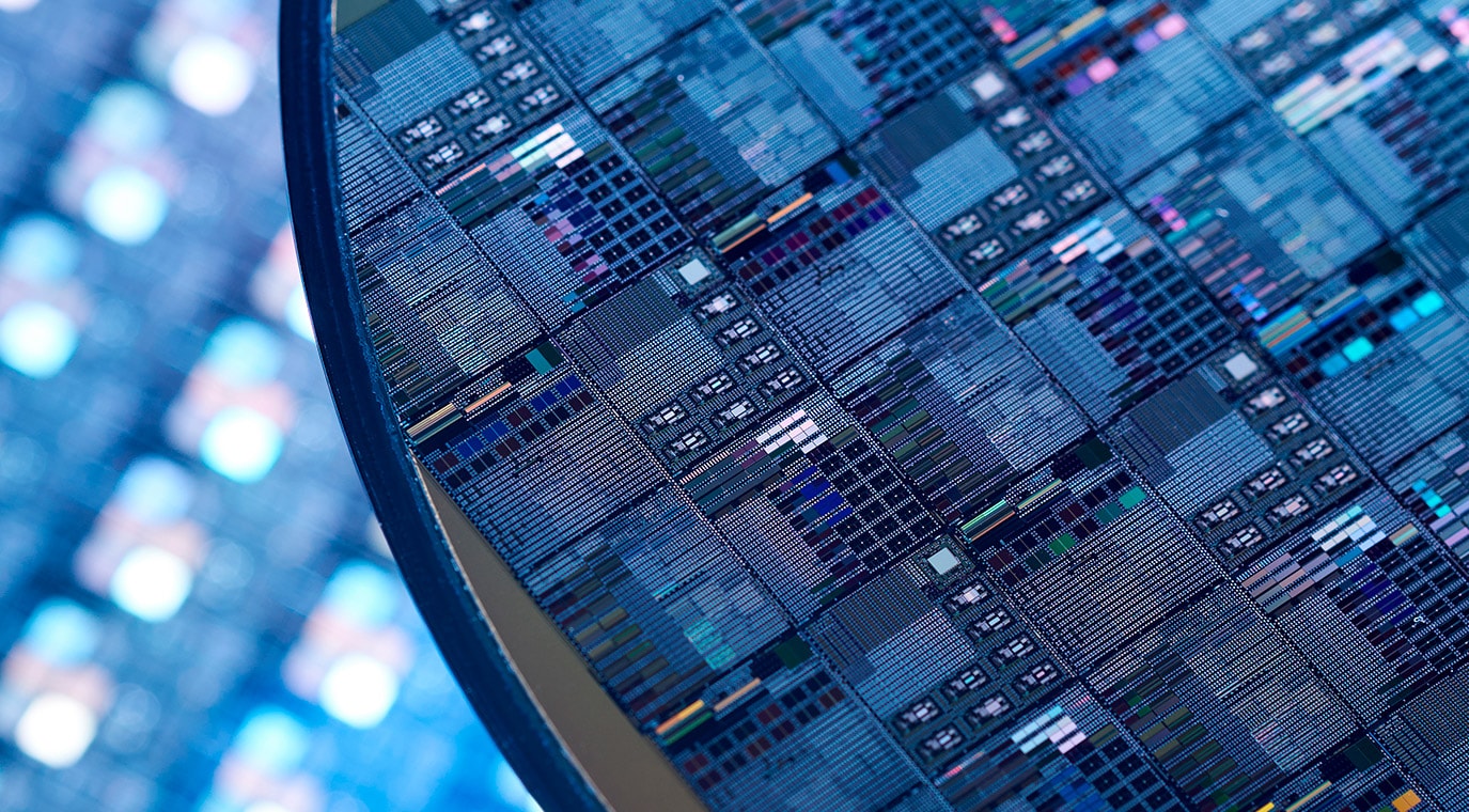
An example of a state-of-the-art semiconductor IC chip is shown in Figure 1, in which 61 billion transistors are integrated. It has a complex pattern just like a map of Tokyo.
The circuit pattern is so finer that it is almost invisible.

- [Fig. 1] An IC chip integrating 61 billion transistors.
- The AI chips integrating GPUs, CPUs and other peripherals continue to evolve for future.
Source: Intel
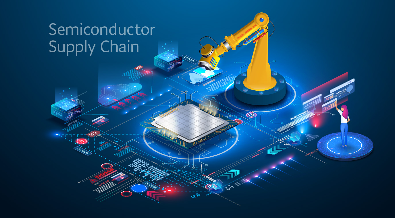
Entire Semiconductor Supply Chain
The production process of an IC chip begins with design, followed by manufacturing of the integrated circuit. Once the fabrication process of an IC chip is completed, external terminals of the device are connected to terminals of the lead frame or substrate before sealing, and the chip is molded by plastic resin. Finally, the entire process of an IC product is completed. The production flow is shown in Figure 2.

- [Fig. 2] The entire semiconductor supply chain
- Created by Kenji Tsuda
- For more information on the foundries, see “What are ‘Foundries,’ the Heroes of Our Times?” in TELESCOPE magazine (Japanese content).
Details of the basic operations of each process and supply chain will be described from the next chapter.
Design Process

- [Fig. 3] Design processes and suppliers
- Created by Kenji Tsuda
Basic operations of the design process are written out in Figure 3. Automatic computing design is mainly used because the design drawings are so complex. Complex integrated circuits are divided into several circuit blocks. Many pre-designed circuits, where technologies protected by Intellectual Properties (IPs) are used and the circuit itself is sometimes called an IP, are assigned to form circuits on a silicon. There are a lot of interconnect wires connecting circuitsin some cases several wires may be in parallel. The basic idea is to be as short as possible. This is to prevent malfunctions caused by signal delay, and/or by signal racing, which many signals in individual lines do not arrive simultaneously . Mainline wirings are called Bus, just like a bus running on a main road, which enables faster signal data transmission and organizes the transmission to prevent collision of transmitted data. It is also necessary to work standardization of software protocols for what data to flow in what order.
In order to enable automatic design, EDA (Electronic Design Automation) vendors of design tools have raised the level of abstraction in upper processes close to the system design, making the IC designer design almost like a programming task. Therefore, debugging is also essential. To verify that the “Program” or the design is correct, simulations are leveraged to see if desired performance and functions are obtained correctly. In the design process, EDA vendors provide design tools, and designers design a circuit with those tools on a computer.
Manufacturing Process

- [Fig. 4] Suppliers of the manufacturing processes
- Created by Kenji Tsuda
Basic operations of the manufacturing processes are as shown in the Figure 4. A wide variety of suppliers from various industries are involved here. In particular, manufacturing equipment using various components and materials is, in a sense, a large system; the components include a wafer transfer container called a FOUP for charging and discharging wafers into and out from a tool, multiple chambers, plasma equipment, power supply and gas piping, valves, robot arms, and linear guides, which are controlled by microcontrollers and/or SoCs, brain of the system. You may notice that various semiconductors are used to operate the semiconductor manufacturing equipment. When the semiconductor shortage loomed large from 2020 to 21, an anecdote was told that semiconductor equipment cannot be produced because of the shortage of semiconductor chips.
As with the design process, automation of the manufacturing process has also progressed, and automated transporters are installed on the ceilings in advanced memory factories and logic/foundry factories with 300 mm wafers. To prevent invisible sweat and debris (called particles) generated out of a human body every time they breaths, from entering a clean room, people are not allowed to enter a clean room except personnel to monitor and maintain the equipment where possible. Additionally, cleanliness of a clean room is constantly monitored with particle counters. A wide variety of companies including manufacturers of equipment, chemicals, pure water, gas, and materials have entered the chip manufacturing market. All of these suppliers are critical for continuing the production, and therefore, avoiding the disruption of the supply chain is essential.
Assembly Process

- [Fig. 5] Suppliers of assembly processes
- Created by Kenji Tsuda
Assembly process is shown in Figure 5. In this process, the received finished wafers are cut into individual chips, the chips are placed on a lead frame or printed circuit, external terminals (leads) are connected to the chip with wire bonding, and then sealed with resin or other material. Fabricated ICs are tested as products after stamping and classified into each category according to their ranks in performance, function, and other specifications, e.g., high-speed, medium-speed, and low-speed products.
Various manufacturing equipment and materials are necessary for mounting the chips in this assembly process as well. For example, elastic tape, where a wafer is placed temporarily for splitting them into chips, is a disposable material used before the chips will be mounted on a substrate. On the other hand, resin that protects the chip is a material that will be used until the end of the product’s life. Either material needs to satisfy strict requirements of the semiconductor manufacturers on its purity and composition.
Countries with Different Expertise in the Process
Overview of the supply chain from an IC user to shipment of the product is shown in Figure 6. Countries of suppliers that have advantages over other suppliers for each step of the supply chain are also shown in the figure.

- [Fig. 6] Overview of the supply chain and countries of suppliers that have advantage for each step
- Created by Kenji Tsuda
For example, companies in the United States, as represented by GAFA, have an advantage over other countries in IT appliances and services that use ICs. China is also strong, imitating the U.S. to develop IT services for its own country. The semiconductor IDMs (Integrated Device Manufacturer) and fabless semiconductor manufacturers in the U.S. are also overwhelmingly strong. Manufacturing equipment makers in the U.S. are also strong, stronger than companies in Japan. Three design tool companies in the U.S. almost monopolize the market, and the only weak points of the country in the supply chain are manufacturing processes, materials, and assembly processes.
Taiwan has an advantage in fabless companies in addition to foundries, with three Taiwanese fabless companies in the global top 10 ranking with American companies. IT services and electronics manufacturers such as Lenovo are the stronghold of China, while they have an advantage only in assembly or the OSAT (Out-sourced Semiconductor Assembly and Test) in the semiconductor supply chain. However, they are gradually strengthening the foundry business as well.
Compared with these countries, Japan’s advantage only lies in the manufacturing equipment makers and the material suppliers with no competitive edge with fabless makers or foundries. However, a new foundry, Rapidus, emerged recently, and globally competitive companies like Sony Semiconductor Solutions, Renesas Electronics, and Kioxia also survived and are growing. Fabless companies used to be more or less subcontractors responding to demands from specific IC users without much room for growth; however, it is encouraging that a company like Socionext is now expanding its business worldwide. Socionext was successful even during the recession in 2023 with its sales from January to September already exceeding the total sales of the previous year by cultivating new overseas customers, just like Japanese manufacturing equipment companies or material suppliers. This is a sign of the advent of a new fabless company that represents Japan.
Why are so many companies involved in the production of a semiconductor chip from design to manufacturing? Logic semiconductors are so complex that it usually takes two to three years before completing a design from scratch, as opposed to approximately three to four months for manufacturing. It was, therefore, natural that a fabless company dedicated to design and a foundry solely for manufacturing semiconductor chips undertake each operation separately instead of one company doing everything. Unfortunately, Japanese companies could not compete in the highly integrated IC market since they stuck to the IDM in which the whole supply chain from design to manufacturing is integrated.
When Dr. Morris Chang, founder of TSMC (Taiwan) looked at fabless startups popped up, one after another in the late 1980s in the U.S., an idea of doing business with them came to his mind, which was, you might say, a natural inspiration. Production of logic semiconductors that require complex designs was divided into fabless and foundry, while conventional IDMs, except Intel, handle memory and analog/power ICs, for which designs are relatively simpler. Additionally, foundries are increasingly used for manufacturing chips, designed for many different types of devices, except mass produced products like memories.
Please refer to The Latest Trends in Semiconductor Fabrication Plants Around the World for an overview of the trends.
Expansion of Semiconductors and the Supply Chain Continues
Companies in the supply chain of semiconductor industry have observed no borders, while political confrontation between the U.S. and China has resulted in fragmentation of the supply chain. However, it would be foolish for any country to withdraw from the semiconductor industry. Growth rate of the industry may not be surprisingly high, but it is steadily growing with an average annual growth rate of 5 to 6%. Applications of semiconductors are expanding, almost limitlessly, from consumer products like home appliances to industrial equipment in, for example, the space/aviation industry, communication industry (e.g., base stations for telecommunications), medical industry, and IT industry with emerging wearable devices.
A symbolic episode was presented on the further expansion of the semiconductor market in the keynote speech at CES 2024 in January 2024. Mr. Nicolas Hieronimus of L’Oreal (France), the world’s largest cosmetics manufacturer, said that cosmetics has been a technology-oriented industry, and has recently started leveraging IT and semiconductor technologies such as generative AI, utilization of various data, and ultrasound and infrared for hair dyeing devices and hair dryers. He also presented a haptics device developed for a physically disabled person which enabled this person to apply lipstick neatly on their own.
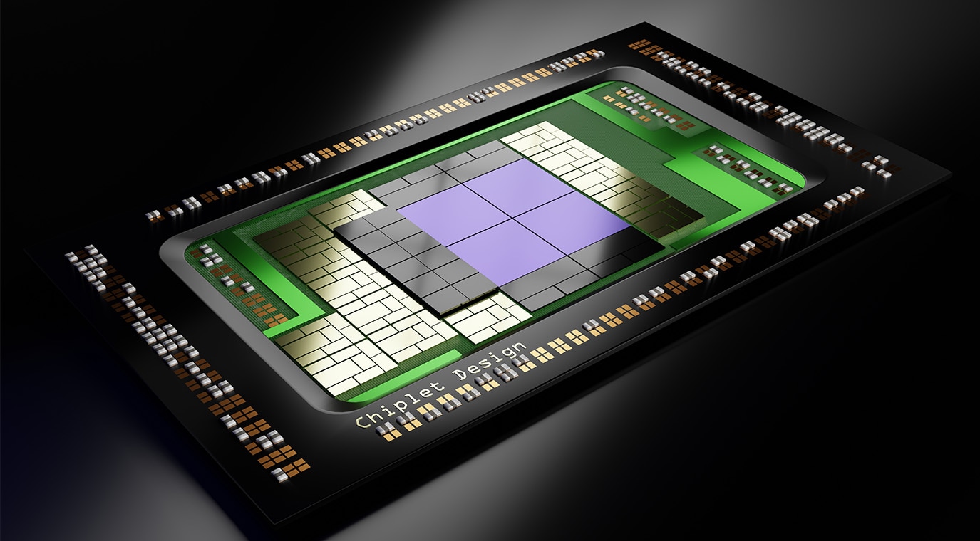
The supply chain will expand increasingly for the years to come since advanced packaging technologies such as chiplet and 2.5D/3D technologies have emerged. Services dedicated to manufacturing and provision of advanced packaging have sprung up globally. NHanced Semiconductor and Silicon Box were founded and started building factories in January of this year in the U.S and August of last year in Singapore, respectively. Intel also opened a factory dedicated to advanced packaging in New Mexico. The electronics industry is beginning to find its way into the mechanical industry as well with the emergence of UCIe, a standards organization for advanced packaging, and the acquisition of Ansys (USA), which provides simulation services for mechanical design, by Synopsys (USA), which develops and sells electronic design software (EDA tools). There is no doubt that the semiconductor industry will see expansion of the supply chain with advancement of specialization.
- #tag
-
- CMOS circuit
- Circuit pattern
- Computer circuit
- EDA vendor
- Fabless Foundry
- IC assembly process
- IC design process
- IC manufacturing process
- IDM
- Integrated circuit
- Logic circuit
- Logic semiconductor
- MOS transistor
- Manufacturing
- Report Series
- Semiconductor
- Semiconductor IC
- Socionext
- Supplier
- Supply chain
- Transistor circuit
- Writer
-
Kenji Tsuda
-
International technology journalist, technology analyst
Kenji Tsuda is a freelance technology journalist who writes both in English and Japanese. With over 30 years of work experience covering the semiconductor industry, Tsuda has been offering various insights to the industry through his blog (newsandchips.com) and analytical articles. He is editor in chief of the Semiconportal site (www.semiconportal.com) and writes the “Car Electronics” article series for Mynavi News site as a columnist.
Tsuda started his career as a semiconductor device development engineer, before becoming a reporter for the Nikkei Electronics magazine at Nikkei McGraw-Hill (now Nikkei BP). At the company, he created several magazines including Nikkei Microdevices (in Japanese), Nikkei Electronics Asia, Electronic Business Japan, and Design News Japan (in English), and Semiconductor International Japanese Edition. Tsuda went freelance in June 2007 as an international technology journalist. Books he authored in Japanese include Megatrend in Semiconductors 2014-2023 (Nikkei BP), Why We Shouldn’t Let Go of the Semiconductor Industry (Nikkan Kogyo Shimbun, Ltd.), The Truth about the European Fabless Semiconductor Industry (Nikkan Kogyo Shimbun, Ltd.), The Latest Trends in Green Semiconductor Technology and New Businesses 2011 (Impress Corp.).
This article is translated by the Nanotech Museum Committee from the original Japanese edition.
(Original article in Japanese)
Recent Articles
Recommended Articles
Loading...
- SHARE!
-
-
-
