JavaScriptが無効になっています。
このWebサイトの全ての機能を利用するためにはJavaScriptを有効にする必要があります。
- Report Series
What is a Chiplet? A Technology That Will Change the Structure of the Semiconductor Industry!
- Text by Motoaki Ito
- 2023.04.26
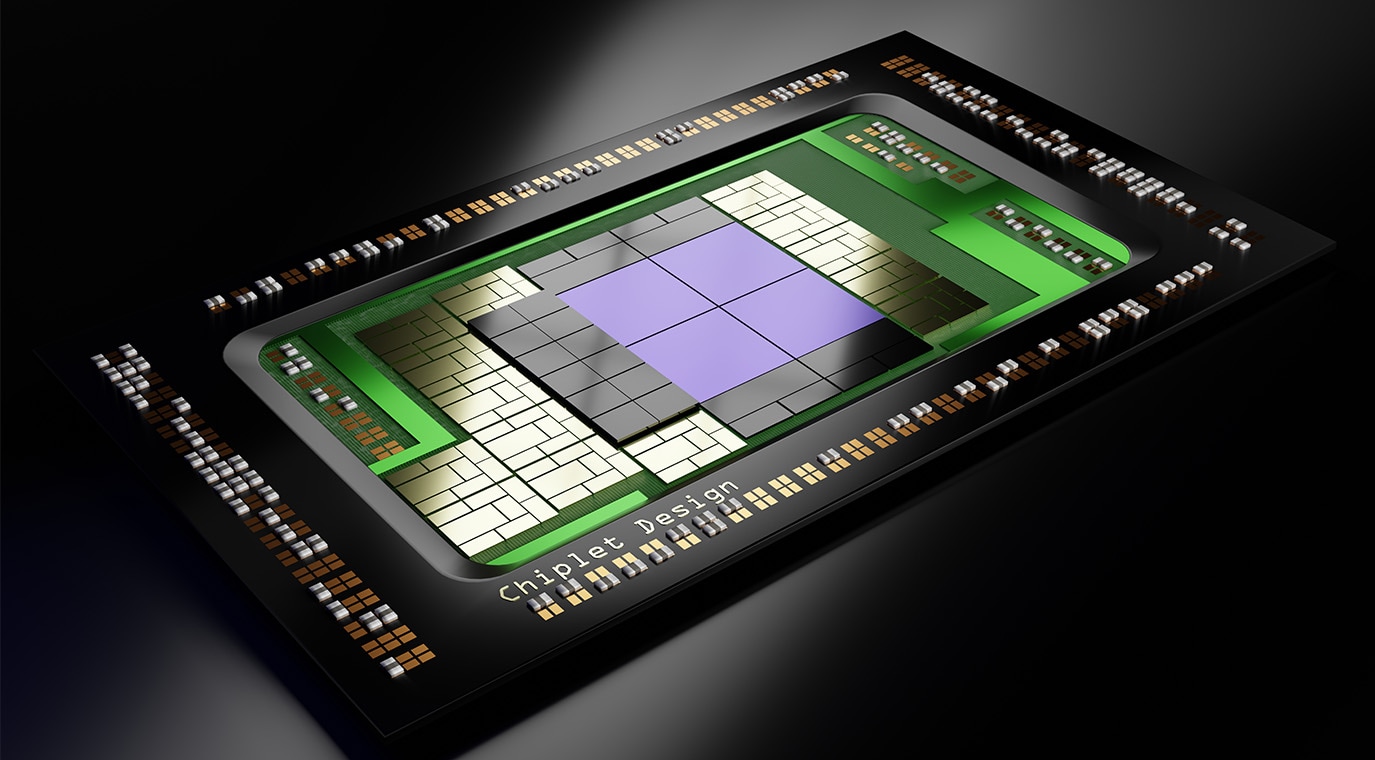
So far, the semiconductor industry has been successful in improving performance, enhancement of multifunctionality, and a reduction in power consumption and cost through scaling of design rules. Technology to reduce design rules was the only thing necessary to enhance the value of a chip without any trade-offs. However, it is becoming difficult to improve yields of semiconductor chips in manufacturing as the scaling of design rules advances in recent years. There were cases where only a limited number of devices could be produced which makes the semiconductor business not viable even if the scaling of design rules was successful. Advances in minite process technologies alone are no longer enough for a bright future for the semiconductor industry. However, a new technologies are emerging to save the industry in this predicament, the chiplet. Applying chiplets not only enables the scaling of design rules to continue to be effective, but also brings new value to the chips. It may transform structure of the semiconductor industry or even change the power structure significantly.
Semiconductors in smartphones, automobiles, and even devices and equipment for national security have become one of the vital elements of modern life, business, and social activities. Electronic devices utilizing semiconductors are indispensable for a sustainable and rich future.
Semiconductor chips have evolved continuously by scaling the design rules of microdevices
integrated on a chip and wiring connecting the circuits. Scaling of design rules of microdevicesand wiring enables integration of larger scale circuits on a small chip, as well as higher performance and lower power consumption of each microdevice. You can also make manufacturing costs lower because larger circuits can be integrated on a smaller chip. In other words, advancement in design rule scaling was a magic method for the evolution of the semiconductor chips without any drawbacks.
In recent years, however, this magic is gradually losing its power. Moore’s Law, an empirical rule that the number of microdevices that can be integrated on a chip increases by two times for every 1.5 or 2 years, is still valid, with some concern for future prospects through the advancement of minite process technologies. However, state-of-the-art minite process technologies are so advanced that the frequency of defects formed during the manufacturing process has become very high, thereby reducing the yield. As a result, manufacturing costs for producing a chip with a certain size have soared, endangering the viability of the semiconductor manufacturers’ business in some cases. Even if the manufacturing of a chip is possible, the price is so high that it cannot be applied widely. This trend becomes even more apparent as the scaling of design rules advances.
What is a chiplet, a technology that integrates a small chip into one package?
There is a new technology that is attracting much attention and expands its application cases to maintain the effects of advancement of the minite process technologies that supports the evolution of semiconductor chips. It is the chiplet (Figure 1). Chiplet technology is a technology where a large scale circuit, which used to be integrated in one chip, is intentionally divided into multiple smaller chips, and accommodates them in one package by mounting them on a substrate called interposer that connects the smaller chips or chiplets. Chiplet means a small chip just like a small baby pig is called a piglet.
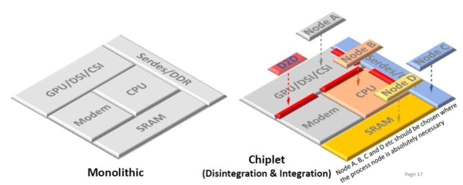
- [Fig. 1] Concept of the chiplet
- Source: SE-Ho You (Samsung), “From Package-Level to Wafer-Level Integration,” IEDM2020, SC1
No chiplet, no advanced semiconductor chips
I would like to explain in detail why the introduction of chiplets, or smaller chips, made by division of large scale circuits enables improvement of yield that otherwise would deteriorate.
Defects will be formed on an arbitrary position on a chip at a roughly constant probability during the manufacturing process with a specific minite process technologies. This is because variations in manufacturing conditions and contamination by impurities and/or inclusion of particles are more or less the same with a specific process technology. As the area of a die (chiplet) increases, the frequency of defective chips also increases, causing the yield to go down. Note that even if only part of a chip is defective, the whole chip will fail.
Dividing a large circuit into multiple smaller circuits to form chips or chiplets before integrating the chips provides better yield than forming a large scale circuit having a large chip area. This is because not only the yield of each chip is higher, but you can also select known good chiplets to form a large circuit.
It has been shown quantitatively at semiconductor conferences that it can actually improve yield (Figure 2). Whole circuitry for a server chip requires a huge chip with an area of 777 mm2 if it is fabricated on a single chip. If this chip is divided into four chiplets, the area of each chip will be 213 mm2. Initial mass production yield of a chip formed with chiplets improves to 21% from 4% when all the circuits are integrated in one chip.
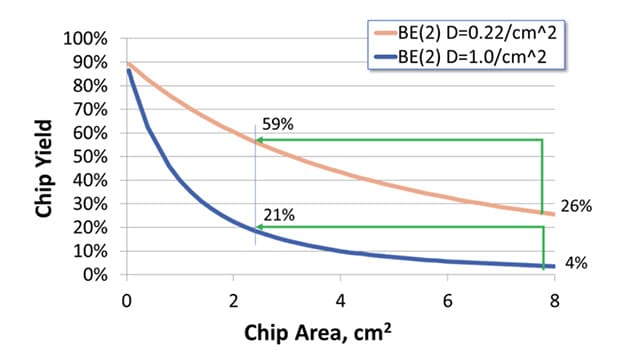
- [Fig. 2] Chip area vs production yield
- The curve shown in blue is the data from initial mass production and the curve shown in orange is when production matures.
Source: Greg Yeric, arm community, “Three Dimensions in 3DIC - Part I,” April 2, 2018
Yield when production becomes mature further increases to 59%, while that for one chip integration is 26%. The number of chips that can be cut out from a single wafer increases to 273 with chiplets, as opposed to 69 with one chip integration. The number of good chips obtained from a single wafer when production matures can be calculated as 69 × 26% = 17 with one chip integration, which increases to 273 × 59% ÷ 4= 40 when chiplet technology is used because four chips are necessary to form an equivalent circuit structure. Number of chips that can be put on the market is more than two times greater with chiplets compared with conventional one chip integration. The difference in profitability at mass production is apparent.
Enables mixed mounting of different types of circuits and chips from other manufacturers, as well as 3D stacking
There are various advantages with chiplets other than the yield enhancement.
Large scale circuits combining chiplets with different process nodes (generations of minite process and different process technologies of logic, memory, analog ICs, RF circuits, power semiconductors, etc., can be accommodated in one package. This technology is called the Hetero-Integration (HI) (Figure 3).
All the circuits integrated on an advanced semiconductor chip have been manufactured with the advanced technology of one chip integration. However, many of the circuits in CPUs or SoCs (System on Chip) can achieve the desired performance without the most advanced technology. Making such circuits with state-of-the-art technology may lead to higher costs and lower yields. In addition, some circuits, such as DRAM, flash memory, and RF circuits, are fundamentally different from logic circuits in terms of manufacturing technology, making them difficult to integrate into a single chip, in the first place. If all the circuits on a chip are manufactured separately according to their characteristics to form chiplets, each chip can be made with best suited manufacturing technologies, which may make it possible further to improve performance, enhance versatility, and reduce costs.
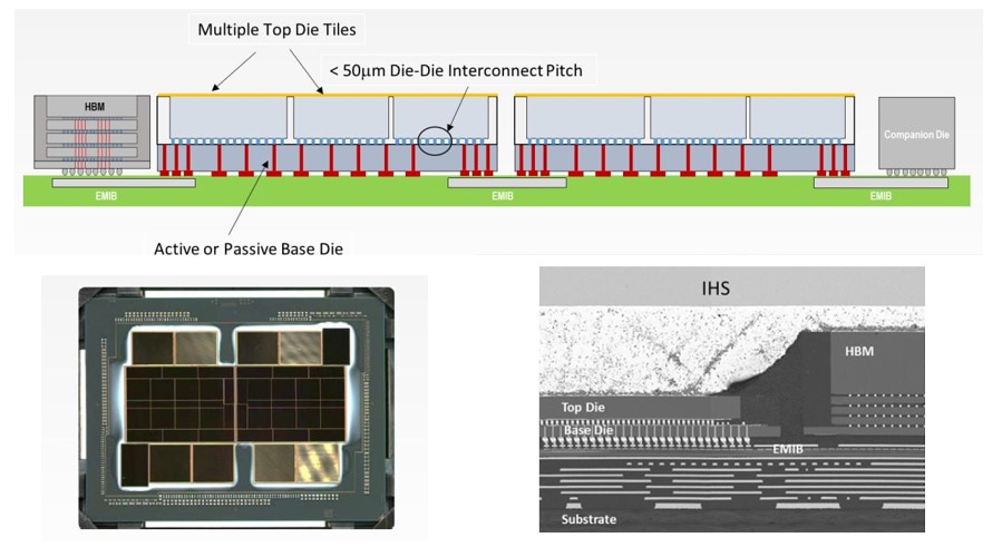
- [Fig. 3] Actual example of the hetero-integration using chiplets
- Structure of mounting technology with GPU Ponte Vecchio of Intel (U.S.) (top), placement of chiplets in the chip (bottom left), and cross sectional view of the chiplets and interposer after mounting (bottom right)
Source: Intel
Large scale chips can also be manufactured by collecting chiplets designed and produced by other companies. To make it easier to take advantage of these benefits, the “UCIe (Universal Chiplet Interconnect Express)” consortium was established to standardize communication methods for chiplet-to-chiplet interfaces and to build an open chiplet ecosystem, and the first specification, “UCIe 1.0,” was released.
Chiplets may transform the structure of the semiconductor industry or even change its power structure significantly
As use of chiplets expands, the structure of the semiconductor industry or its power structure may change significantly.
Conventionally, integration of a large scale circuit with one chip has been assumed with development of advanced semiconductor chips, and, therefore, all the circuits integrated on the chip must be prepared by one company regardless of its own area of expertise. However, if chiplets are used, SoP (System on a Package) combining chiplets from different manufacturers can be developed easily and in a short period of time.
Semiconductor makers that can develop unique chiplets but cannot design large scale chips may become important in the industry. It is also likely that a equipmentmaker develops specific chiplets only, and manufactures applied products that can differentiate the company from competitors. A new type of business that can be called a Semiconductor General Contractor may emerge, where unique chiplets will be collected to develop and manufacture a large scale chip to meet the requirements from user companies. Trends related to chiplets cannot be overlooked when you try to foresee the future of the semiconductor industry.
- Writer
-
Motoaki Ito
-
Motoaki Ito is the CEO of Enlight, Inc. which he founded in 2014. The company leverages its expertise in communicating the value of specific technologies to the target audience, and offers marketing support mainly to technology companies.
Prior to setting up Enlight, Ito worked for Nikkei Business Publications (Nikkei BP) for four years as an advertising producer of its technology information group, with a main focus on marketing support. Before that, he spent six years as a consultant at TechnoAssociates, Inc., a joint think tank between Nikkei BP and Mitsubishi Corporation, supporting the clients' manufacturing operations.
Prior to that, he worked for 12 years as a journalist, editor, and editor-in-chief for various publications including Nikkei Microdevices, Nikkei Electronics, and Nikkei BP Semiconductor Research, after a three-year stint at Fujitsu developing semiconductors as an engineer.
This article is translated by the Nanotech Museum Committee from the original Japanese edition.
(Original article in Japanese)
Recent Articles
Recommended Articles
Loading...


