JavaScriptが無効になっています。
このWebサイトの全ての機能を利用するためにはJavaScriptを有効にする必要があります。
- Report Series
The Latest Trends in Semiconductor Fabrication Plants
Around the World
- Text by Kenji Tsuda
- 2023.12.04
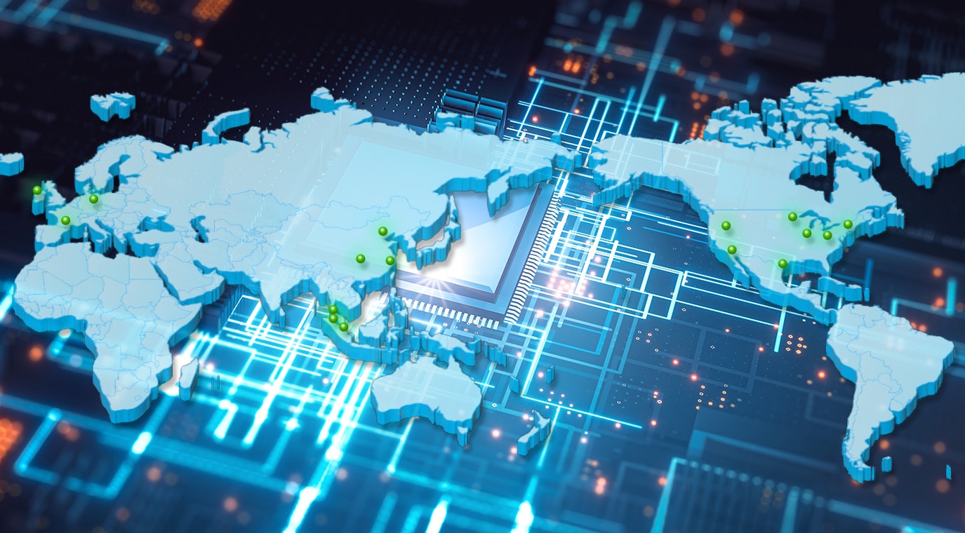
From 2022 to 2023, there has been news that new semiconductor fabrication plants are being built around the world. Starting with TSMC in Taiwan, Intel, Micron Technology, Global Foundries in the United States, Infineon Technologies, Robert Bosch, STMicroelectronics and other European entities will also build new fabrication plants one after the other. They are also trying to build new fabrication plants in Japan, the United States, Europe, and in Southeast Asia such as in Singapore and Malaysia, as well as in China. This is a report on the actual status of the construction of the new fabrication plants worldwide, the reasoning and background thereto, and the future trend.
The semiconductor supply chain is composed of individual industries
Until now, the semiconductor supply chain has been a specialty area for each country, and it has been composed of individual specialties. The top three companies in the United States accounted for the EDA (electronic design automation) tools that are indispensable for semiconductor design. The Taiwanese foundry undertook the fabrication of American fabless companies. There is a global specialties (Fig. 1) in that Japan, the United States, and the Netherlands are strong for the semiconductor manufacturing equipment that is essential for the foundries, and Japan has a strong structure for semiconductor materials.
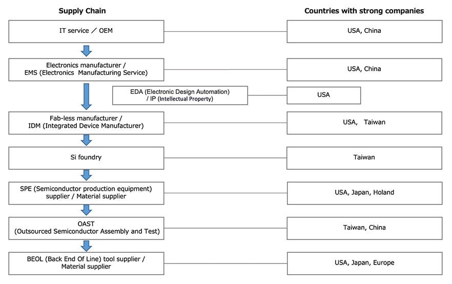
- [Fig. 1] Semiconductor Supply Chain
- Created: Kenji Tsuda
The individual countries in the supply chain is about to change
Such a specialty in the global supply chain is beginning to collapse because of political factors. Conversely, it can be said that this is because countries around the world have begun to recognize the value of the semiconductor industry. The phrase “solving social problems with technology” is being used around the world. If we stick to the technology that solves social problems, we will always end up in semiconductors.
For example, in the fall of 2022, Akira Shimada, President of NTT, made it clear at a media event at the company’s Musashino Research and Development Center that “the IOWN*1 initiative could not be attained without the cooperation of semiconductor manufacturers.” Intel’s CEO, Pat Gelsinger, stated at the company’s new plant launch in Ireland that “everything (socially and economically, and the like) is digital, and a silicon-based society and economy are called Siliconomy.”
As the impact of semiconductors has spread to society and the economy, it has also expanded to industries such as aerospace and defense, and has developed into a political issue.
A new trend has emerged to handle both design and manufacturing in various countries, that until now had been individual specialties in which semiconductor design was done in the United States and manufacturing was done in Taiwan. The United States, which has not been very good at manufacturing until now, is beginning to focus especially on semiconductor manufacturing. There is also a movement to build new fabrication plants in Europe, and there is also an active movement in Asia other than South Korea and Taiwan, where semiconductor manufacturing has been active so far (Fig. 2).
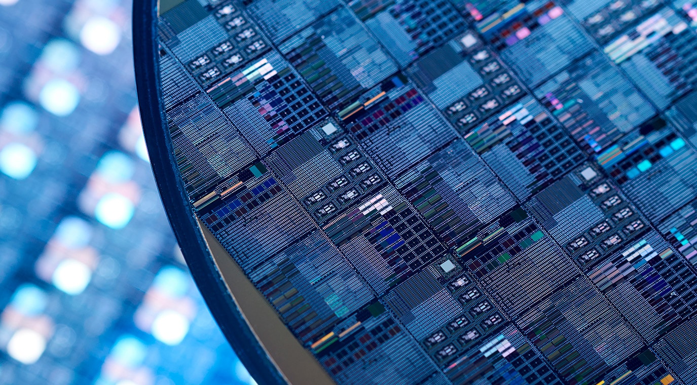
A list of semiconductor fabrication plants around the world

Countries that focus on fabrication plants have three features. Firstly, they set up a fabrication plant in their country to secure semiconductor chips. Secondly, they attract fabrication plants from foreign companies. Thirdly, production capacity is expected to increase in anticipation of the growth potential of semiconductors.
US construction rush focused on semiconductor manufacturing
Intel, long the world leader in semiconductors, has its main fabrication plants in the states of Arizona and Oregon, but is expanding its existing plants in Arizona and building a new one, the Fab 42. It is connected to the existing factory through a communication corridor, and the distance from the end to the end is said to reach 1.6 km. Intel is investing $30 billion in the new Arizona plant with the Canadian asset management company Brookfield.
Furthermore, in September 2023, construction began on a huge fabrication plant in Ohio, where has so far had little to do with semiconductors. They plan to invest $100 billion in Ohio over 10 years to build eight fabrication plants. They released a video of the construction of the first fabrication plant.
Micron Technology, the third largest memory manufacturer and IDM, began building a new fabrication plant in Boise, Idaho, in October 2023. Micron plans to invest $15 billion over the next 10 years.
GlobalFoundries, the largest foundry in the United States, already has a plant in Malta, near Albany, New York, where its semiconductor research and development is located, and it has relocated its headquarters there. In July 2021, GlobalFoundries announced that it would build a new plant near Malta, but in April 2023, GlobalFoundries finally acquired 800 acres of land (equivalent to about 70 Tokyo Domes). Several years ago, it was pointed out by analysts and others that GlobalFoundries was no longer focusing on production in the United States, but they indicated a policy to expand their production scale and new plants in the United States in order to reclaim their honor.
A few years ago, Skywater Technology, which specializes in the foundry business for American companies, acquired the former Cypress Semiconductor fabrication plant in Bloomington, Minnesota, and began to focus on the foundry business. It has received orders from the Pentagon and has called itself Trusted Semiconductor Manufacturer to differentiate itself from other foundries. It has also made PDKs (process development kits) focusing on 130 nm and 90 nm to attract customers. Furthermore, it announced the construction of a new plant on the campus of Purdue University in Indiana, and has partnered with 12 universities in Ohio, Indiana, and Michigan to build a network to send semiconductor talent all over the US chip industry.
Skywater Technology is also an SoC manufacturing plant that uses open-architecture RISC-V processors with Google initiative. Google is developing a business model that will attract semiconductor users, and will design at the semiconductor design company eFabless, and manufacture at Skywater Technology.
The United States is also actively attracting foreign companies, and has attracted TSMC to Arizona and is currently building plants. Here, the 5-nm process aims to be operational by 2024, but equipment from ASM and ASML in the Netherlands, Applied Materials, Lam Research, and KLA in the United States, and Tokyo Electron in Japan have already been delivered. However, there are reports that securing talent to work in the semiconductor industry domestically is difficult; operations may be delayed to 2025 years.
At TSMC’s Arizona plant, there is also talk of building a second plant, which is thought to be a 4 nm/3 nm process line. South Korea’s Samsung has a foundry in Austin, Texas, and it has announced plans to build a new one in Taylor, about 30 kilometers away.
In European countries, the construction of new fabrication plants is ongoing
Intel completed a new plant in Ireland at the end of September, 2023. The plant is an “Intel 4” process mass production plant; photos of the inside have already been released (Fig. 3). They originally entered Ireland in 1989 and have invested 30 billion Euros to date.
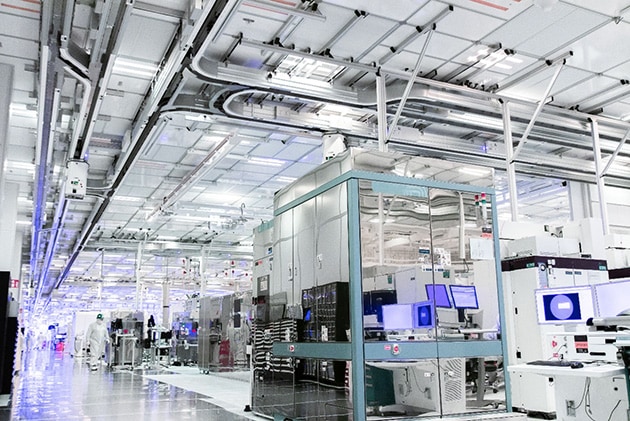
- [Fig. 3] New Plant in Ireland Unveiled by Intel at the End of September, 2023
- Source: Intel Corporation
In addition to Ireland, Intel has announced that it will build a process plant in Dresden, Germany, and a packaging plant in Poland. Dresden was also the headquarters of GlobalFoundries. It is equipped with manufacturing equipment, gas, water and other equipment facilities, making it easy to build a semiconductor manufacturing plant.
STMicroelectronics, in collaboration with GlobalFoundries, signed a contract in June, 2023 to build a 300-mm wafer processing plant in Crolles, near Grenoble, France. The two companies will jointly operate; the total cost is expected to be 7.5 billion Euros. Both use FD-SOI (Fullly depleted silicon on insulator) technology, so an ecosystem is available.
In September 2021, Infineon Technologies built a 300-mm wafer power semiconductor plant in Villach, Austria, and began construction of a second 300-mm mass production plant in Dresden, Germany, as early as May 2023. A 300-mm plant is already in Dresden, but it was only a small-scale, pilot line.
Like Intel, TSMC chose Dresden as its manufacturing base in Europe. Germany’s Robert Bosch, Infineon Technologies and the Netherlands’ NXP Semiconductors will also make investments, bringing total investments to more than 10 billion Euros. Construction of the TSMC plant will begin in late 2024; production is scheduled to begin by the end of 2027. Europe, like Japan, has strong automotive and industrial fields, so no process below 7 nm is required. They plan to have the same 22/28 nm and 16/12 nm processes as the Kumamoto plant in Japan.
In Asia, Singapore is particularly enthusiastic to lure semiconductor industries
South Korea and Taiwan are still focusing on manufacturing plants. In Asia, excluding South Korea, Taiwan, and Japan, Singapore is booming in the construction of semiconductor process plants.
GlobalFoundries began construction of their new plant in 2021, and opened their 300-mm process plant in September, 2023. It is said that 110,000 FOUPs are in production daily. GlobalFoundries has an existing plant in Singapore, and are adding a new plant for 450,000 wafers per year to a total Singapore plant of 1.5 million wafers per year.
UMC (Taiwan), which already has a manufacturing plant in Singapore, announced the construction of a new plant in February, 2022, following Micron Technology’s expansion of their new NAND Flash plant in 2019. They have invested $5 billion and they are planning to start production in 2024.
Singapore’s Silicon Box completed its advanced packaging*2 plant using chiplets*3 in July 2023. They have invested $2 billion to build a cleanroom comparable to a process plant. In a graphics video that shows the inside, they have a system that automatically conveys containers like FOUP equipped with wafers, carrying a large number of substrates on a ceiling rail; it seems like a process factory.
Intel and Infineon Technologies are focusing on Malaysia, and Intel announced in August, 2023 that it would build an advanced packaging plant that uses 3D chips. They plan to invest $7 billion in the Malaysian plant over the next 10 years. In August, 2023, Infineon Technologies announced that it will build a process plant for SiC power semiconductors in Kulim, near the opposite shore of Penang Island. Micron Technology completed expansion of their NAND Flash packaging plant in October, 2023, and has invested $1 billion to date.
At present in China, Samsung’s Xian plant, SK Hynix’s (South Korea) Wuxi and Dalian plants, and TSMC’s Nanjing plant are currently mass-producing, accounting for the majority of manufacturing in China. Chinese companies have also gained strength recently. SMIC, the top foundry, has a large plant in Shanghai, but Reuters reported on August 26, 2022 that SMIC plans to build a 300-mm plant in Tianjin. Plans to produce 100,000 wafers per month in the 28 nm to 180 nm process.
There is also news that SMIC has successfully developed a 7 nm process. The “Kirin 9000s” mobile processor mounted on Huawei’s smartphone “Mate 60 Pro” is manufactured in the 7 nm process at SMIC; the Canadian market research company TechInsights disassembled and analyzed it. If the information that the number of integrated transistors is 89 million is true, it is conceivable to see this as a 7 nm process. The number of transistors in TSMC’s 7 nm process is 90 million. There is virtually no wiring width of 7 nm, and the minimum dimension of the chip called the 7 nm process is 15 to 16 nm; the name of the process is 7 nm and 5 nm from the number of transistors per area.
Furthermore, YMTC (China), which produces NAND flash, announced 232-layer products in December, 2022. However, it was put in a difficult position because the United States announced that it was on its entity list. However, it has also been reported in April, 2023 that products were produced with Chinese equipment, and that they are being shipped as SSDs in cooperation with domestic SSD manufacturers.
In the future, also pay attention to what is going on in India and Vietnam
We have seen new semiconductor fabrication plants in the United States, Europe, Asia, and the world, but it looks like the semiconductor industry is going to wake up in India and Vietnam in the future. India has been strong in semiconductor design since the 1990s, and semiconductor design has begun in Vietnam. Together, they are beginning to find value in manufacturing.
[Footnote]
- *1 IOWN
- TELESCOPE magazine What is IOWN and photoelectric fusion technology in the 200th year of the revolution in communication infrastructure? (Japanese content) Reference
- *2 Advanced packaging
- The leading-edge package represents the physical packages themselves, and leading-edge packaging represents the packaging technology. An advanced packaging plant is a plant that makes advanced package products.
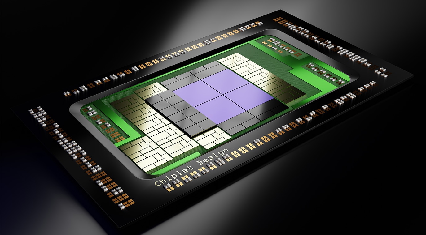
- *3 Chiplet
- TELESCOPE magazine What is a Chiplet? A Technology That Will Change the Structure of the Semiconductor Industry! Reference
- #tag
-
- Robert Bosch
- ASM
- ASML
- Applied Materials
- GlobalFoundries
- Google eFabless
- Huawei
- Infineon Technologies
- Intel
- KLA
- Lam Research
- Manufacturing
- Micron Technology
- NTT
- RISC-V
- Report Series
- SK Hynix
- SMIC
- STMicroelectronics
- STMicroelectronics NXP Semiconductor
- Samsung
- Semiconductor
- Semiconductor fabrication plants
- Silicon Box
- Skywater Technology
- TSMC
- UMC
- YMTC
- Writer
-
Kenji Tsuda
-
International technology journalist, technology analyst
Kenji Tsuda is a freelance technology journalist who writes both in English and Japanese. With over 30 years of work experience covering the semiconductor industry, Tsuda has been offering various insights to the industry through his blog (newsandchips.com) and analytical articles. He is editor in chief of the Semiconportal site (www.semiconportal.com) and writes the “Car Electronics” article series for Mynavi News site as a columnist.
Tsuda started his career as a semiconductor device development engineer, before becoming a reporter for the Nikkei Electronics magazine at Nikkei McGraw-Hill (now Nikkei BP). At the company, he created several magazines including Nikkei Microdevices (in Japanese), Nikkei Electronics Asia, Electronic Business Japan, and Design News Japan (in English), and Semiconductor International Japanese Edition. Tsuda went freelance in June 2007 as an international technology journalist. Books he authored in Japanese include Megatrend in Semiconductors 2014-2023 (Nikkei BP), Why We Shouldn’t Let Go of the Semiconductor Industry (Nikkan Kogyo Shimbun, Ltd.), The Truth about the European Fabless Semiconductor Industry (Nikkan Kogyo Shimbun, Ltd.), The Latest Trends in Green Semiconductor Technology and New Businesses 2011 (Impress Corp.).
This article is translated by the Nanotech Museum Committee from the original Japanese edition.
(Original article in Japanese)
Recent Articles
Recommended Articles
Loading...
- SHARE!
-
-
-
