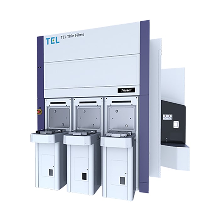
Deposition Triase+™Series
Designed to deliver optimal solutions for a wide range of challenging thin film depositions.
The Triase+™ series offers extra value as the latest single wafer deposition system, by allowing direct incorporation of various 300mm processing modules. The Triase+™ series predominately or primarily provides high precision metal deposition process such as Ti, TiN and W for plug and electrode formation with excellent tool reliability. In addition to the metals, Triase+™ SPAi for low temperature plasma processing system provides a wide range of critical FEOL applications. The Triase+™ series has been applied over the years with an extensive product lineup to suit each and every customer production requirements.

Semiconductor process technology has been continually scaling down and moving toward 3D structures, that present challenges in the film deposition. The Triase+™ ™ EX-II™ TiN (Titanium Nitride) is an advanced 300mm single wafer deposition system for high speed ASFD*1 which enables high-quality thin film formation with excellent within-wafer uniformity and high step coverage characteristics. Featuring an optimized reactor design with new gas injection module, the system achieves high productivity even in the leading-edge semiconductor device manufacturing, and is used for various applications including formation of contact barriers, capacitor electrodes, word line barriers and metal gates. The Triase+™ EX-II™ TiN Plus provides excellent uniformity for conformal metal deposition of TiN on complex structures. Also, two of the latest models have been added to the line-up. The Triase+™ EX-II™ TiN Plus HT specializes in high-temperature TiN deposition that is aimed to gain lower contact resistance film with reducing impurity levels, whereas the Triase+™ EX-II™ TiON (Titanium OxyNitride) provides low leakage current TiON film deposition with can be used in MIM capacitor*2 electrode formation. All these models have flexible design, up to four chambers can be integrated and individual chamber has optimized clean technology to achieve high productivity and low CoC.
*1 ASFD: Advanced Sequential Flow Deposition. A low-temperature processing method for forming nanoscale metal films with highly-engineered properties
*2 MIM capacitor: Metal-Insulator-Metal capacitor. It consists of two metal layers with an insulator layer in between
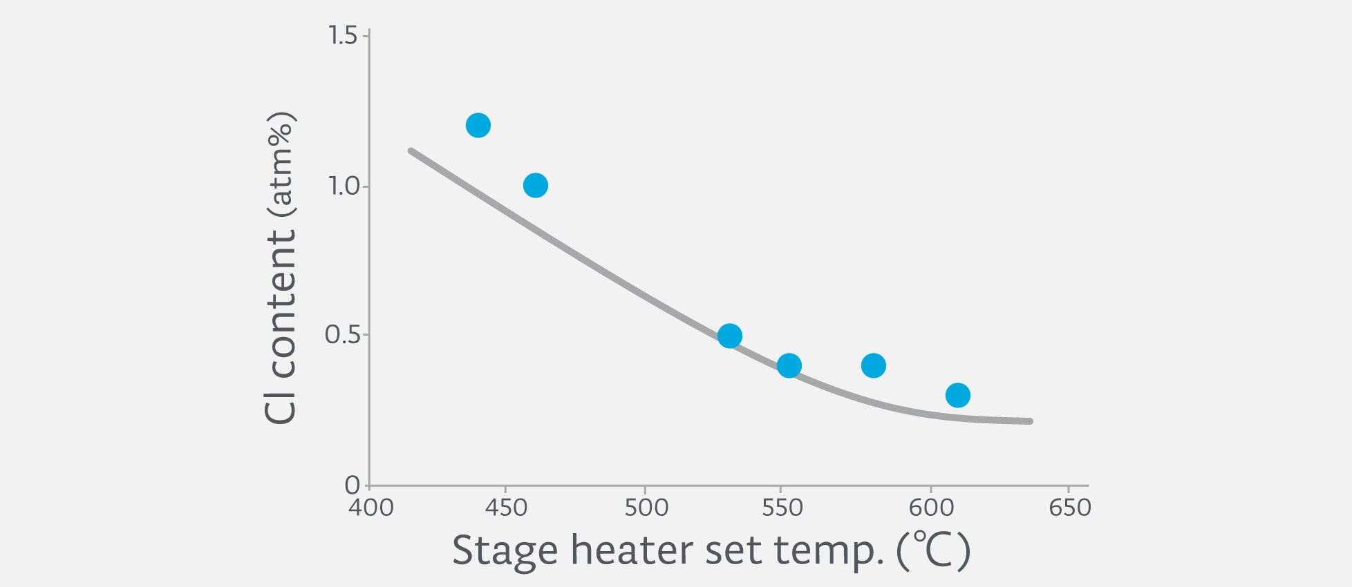
TiN film Chlorine content
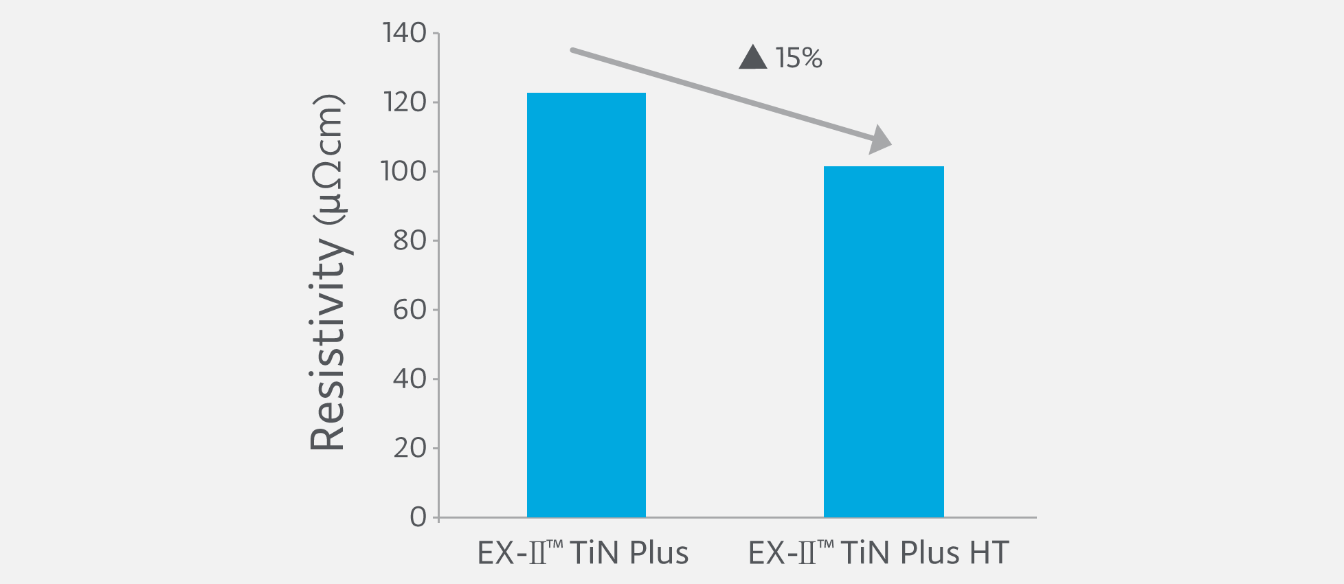
TiN film resistivity reduction
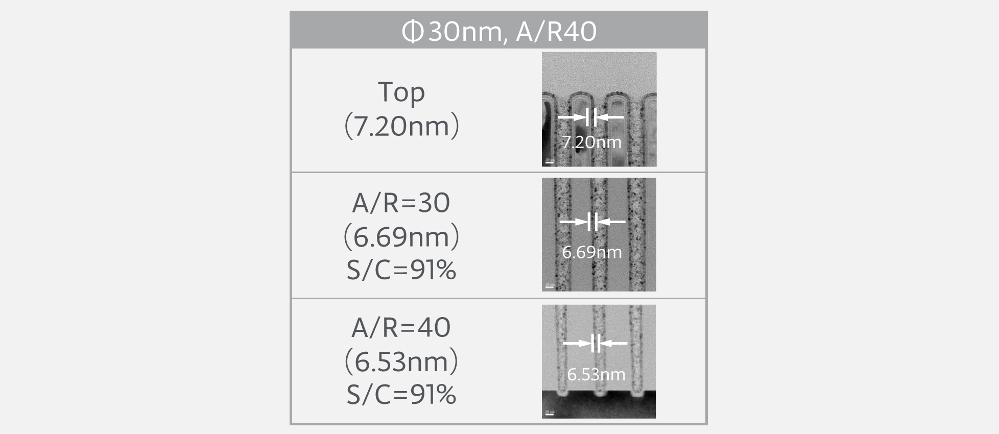
EX-Ⅱ™ TiN Plus HT coverage
Triase+™ Ti/TiN is a 300mm single-wafer metal CVD system for high step coverage Ti/TiN film formation using TiCl4. Based on TEL's industry-proven Trias™ platform, since its introduction, the system provides low contact resistance film process while reducing contact leakage of various devices. Especially in high-aspect-ratio contact hole, Triase+™ SFD™ TiN has been widely adopted by using SFD™ technology that has both merits of excellent step coverage of ALD and high productivity of CVD. The Triase+™HP Ti, single-wafer metal CVD system, accommodates a lot of additional functions such as optimized surface treatments by unique showerhead gas dispersion module and simultaneous TiSix formation technology during Ti deposition. Furthermore the system provides widen temperature control range, lower particle level and higher productivity. Its unique technology addresses the various process requirements of metal deposition that having the structure such as ultra-shallow junction and nickel silicide contacts. As a successor model, Triase+™ HP Ti Plus, which allows higher step coverage for next generation devices, has also been added to the product lineup.

Triase+™ W is a 300mm single-wafer CVD system that delivers high step coverage tungsten (W) film deposition using WF6. By combining rapid heat up and cool down of wafer temperatures and with plasma-less chamber cleaning technology, the system achieves higher productivity and lower CoO. Utilizing SFD and CVD methods respectively, the Triase+™ W provides in-situ deposition of both nucleation and bulk film. This ensures high step coverage, even with small geometry, contact holes. The system is also capable of depositing low-resistance film to meet further scaling needs, and is suitable for such applications as contact plug formation and via filling.

Triase+™ SPAi, a successor to the production proven and highly reliable Trias™ SPA series, was developed in response to the market’s demand for higher productivity and reduced environmental loads. The Trias™ SPA series featured the Slot Plane Antenna technology that TEL has been developing over the years, which generates high-density, low-electron temperature plasma to enable, low-damage, low-temperature plasma processing. The Triase+™ SPAi system inherits its predecessors’ reliability, to equally enhance system throughput, achieve higher productivity, lower power consumption (which reduces CO2emissions), and a smaller footprint. An integrated bias function helps to produce high quality film while maintaining excellent coverage, and making the system suitable for critical FEOL applications including gate nitridation, gate recovery oxidation, STI liner oxidation, and high-k nitridation.
Product comparison
 |
 |
 |
 |
|
| Wafer size (mm) |
300 | 300 | 300 | 300 |
| Availability | Certified used | Certified used | Certified used | Certified used |
| Application | Capacitor electrode, Word line barrier, Metal gate |
Contact, Capacitor electrode |
Contact plug, Via Fill |
Gate nitridation, Gate recovery oxidation, STI liner oxidation, High-k nitridation |
| Process | ASFD TiN, TiON | CVD Ti/TiN | W | Oxidation, Nitridation |
| Substrates | Si | Si | Si | Si |
| Additional features | High step coverage, Good TiN film property, High speed deposition, Cycle time, ClF3 cleaning |
High step coverage, Simultaneous TiSi, Formation during Ti deposition, ClF3 cleaning |
High productivity, ClF3 cleanining |
Low tempreture and damageless plasma process, High density and low electron tempreture plasma |
Triase,Triase+,EX-Ⅱand SFD are registered trademarks or trademarks of Tokyo Electron Group in Japan and/or other countries.
