Tokyo Electron Develops Memory Channel Hole Etch Technology That Enables Ultra-fast 10-µm-deep Etching for 3D NAND Flash with Over 400 Layers and an 84% Reduction of Global Warming Potential
Tokyo Electron (TEL; Head Office: Minato-ku, Tokyo; President: Toshiki Kawai) announced that its development team at Tokyo Electron Miyagi—the development and manufacturing site for its plasma etch systems—has developed an innovative etch technology capable of producing memory channel holes in advanced 3D NAND devices with a stack of over 400 layers. The new process developed by the team has brought dielectric etch application to the cryogenic temperature range for the first time, producing a system with exceptionally high etch rates. The innovative technology not only enables a 10-µm-deep etch with a high aspect ratio* in just 33 minutes, but also can reduce the global warming potential by 84% compared with previous technologies. The geometry of the etched structure is quite well-defined as shown in the figure 1. Potential innovations enabled by this technology will spur creation of 3D NAND flash memory with even larger capacity.
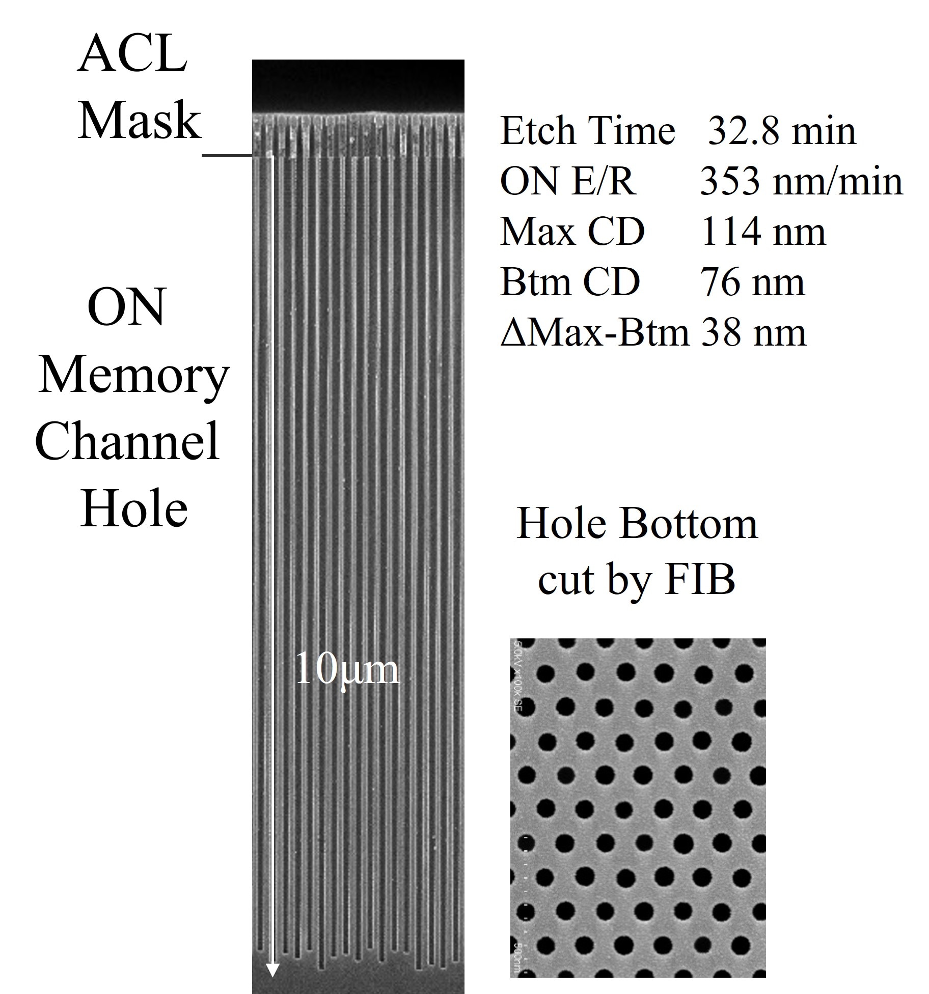
Fig1. Cross section SEM image of memory channel hole pattern after etching, and FIB cut image at the hole bottom.
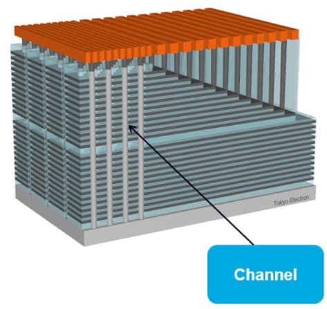
Fig.2 3D NAND Flash
TEL’s team that developed this technology will present a report on its research results at the 2023 Symposium on VLSI Technology and Circuits, one of the most prestigious international conferences on semiconductor research, to be held from June 11 to June 16 in Kyoto. Please look forward to our technology presentation that contributes to semiconductor technology innovation and global environment protection.
Continuing to pursue the motto of Best Products and Best Technical Service, TEL will contribute to technological innovation in semiconductors. As this year marks the 60th anniversary of our founding—which we consider to be a new transformative point for us—we will take on new challenges and continue to evolve, contributing to the development of a dream-inspiring society.
*Aspect ratio: Depth to width ratio of the pattern formed on the wafer.
Presentation title:
Beyond 10 µm Depth Ultra-High Speed Etch Process with 84% Lower Carbon Footprint for Memory Channel Hole of 3D NAND Flash over 400 Layers
Y. Kihara, M. Tomura, W. Sakamoto, M. Honda and M. Kojima,
Tokyo Electron Miyagi Ltd.
Session, date and time of presentation:
Technology Session 3, NAND Flash [Shunju II]
Tuesday, June 13, 2 p.m. - 3:40 p.m.
Click here for detailed event information.: 2023 Symposium on VLSI Technology and Circuits
The copyright to the paper to be presented at the conference, including that for ancillary material such as photos in Figure 1, belongs to the Japan Society of Applied Physics. For inquiries regarding the use of the material concerned, please contact the secretariat of the 2023 Symposium on VLSI Technology and Circuits.
VLSI Secretariat
Japan and Asia
vlsisymp@jtbcom.co.jp
