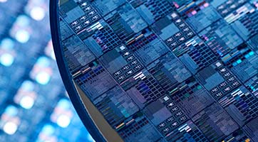


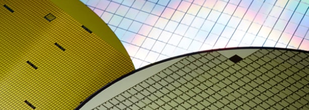
- Semiconductor Technology Now
Expert Interview
 |
Telescope Magazine: What’s the difference between a quantum computer that performs massively parallel processing and that for solving quantum annealing problems?
Masanao Yamaoka: The type of quantum computer that solves problems by means of massively parallel processing is called the logic gate quantum computer. This is also a very important technology, of course. Since it is not specialized to solve optimization problems, however, work is needed to make it more universal so it can replace conventional CPUs. We at Hitachi are also working to develop quantum gate computers at the Hitachi Cambridge Laboratory in the U.K. This significant effort will hopefully become fruitful in the not-too-distant future.
Quantum gate computing currently has two major issues. The first one is that of scale: for a quantum gate computer to perform well, it has to be sufficiently large in scale. Google has recently developed a 72 quantum bit (qubit) computer chip, but more work is needed before something larger in scale comes along for practical use. The second issue is that of algorithm. While Peter Shor’s algorithm (for integer factorization) and some other search algorithms have been announced for quantum computing, many more need to be developed before the technology becomes more universal. I imagine it would take much longer than four or five years to get there.
Telescope Magazine: Meanwhile, CMOS annealing technology is threatened by the imminent end of Moore’s Law. How do you plan on coping with this problem?
Masanao Yamaoka: Our CMOS annealing technology is inherently scalable as it is based on digital circuits, so we can simply connect many chips to achieve horizontal scaling. I think we can make the system much larger as time goes by.
We can even make CMOS annealing chips go 3D. Because so many people are working on semiconductor technology, they won’t easily let the limitations of Moore’s Law put an end to the entire industry.
Telescope Magazine: What other applications are there for CMOS annealing?
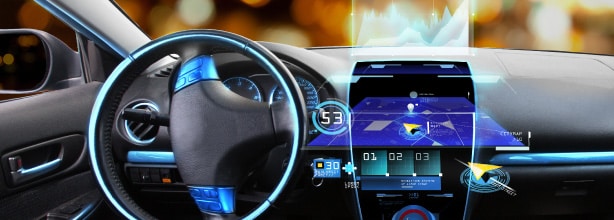
Masanao Yamaoka: Possible applications are endless. The technique can be used to solve such problems as frequency allocation for mobile stations, optimal prioritization of inter-drone communication, securing robustness of communication network, image recovery, and speedy detection of explosives. Scheduling problems are another area this technique can be applied: generating brackets for high school baseball tournaments, organizing shifts for factory workers, developing staffing schedule for restaurants, and so forth.
Process optimization is an integral part of AI. However, AI cannot optimize a solution without a set of accumulated data. That is where quantum annealing comes in. It is a technique best suited to solving the current optimization problem in real time.
Telescope Magazine: What are your plans going forward?
Masanao Yamaoka: Our development efforts are geared toward making CMOS annealing available for various applications, so we are racking our brains to make the technology more practical to use. We are on the lookout for potential corporate users who are willing to conduct joint verification tests with us.
We also need to expand the user base, so we are considering producing a software development kit (SDK) and bundling it with CMOS annealing circuits and FPGA boards. The plan is to develop the first version of SDK at Hitachi, then releasing it to obtain user feedback for further improvement.
As a means to solicit ideas from the public about new combinatorial optimization applications, we conducted two programming contests for a CMOS annealing machine jointly with the Research Institute for Electronic Science (RIES) of Hokkaido University last year. The number of programmers registered in the contest is roughly 1,000. The contest is not for applications per se, but rather for conversion programs that enable the CMOS annealing machine to handle the applications. The contestants are extremely talented, so we would very much like to keep in touch with them and ask for their cooperation.
Ideally, we would do well to incorporate this technology into Lumada*9, Hitachi’s IoT platform for digital transformation. Among other things, Lumada brings OT (operational technology) and IT (information technology) together, optimizing factory efficiency and reducing downtime. So, CMOS annealing technology seems to be a very good fit with Lumada.
|
Footnotes
- *9
- Lumada:
Hitachi’s IoT software platform that comprehensively delivers data collection, management, analytics, and visualization. Actually, Lumada is more than just an IoT platform: it is a far-reaching ecosystem that includes AI and digital transformation for solving social problems.
Reference
- 1.
- Paper presented at ICRC:
Takuya Okuyama ; Masato Hayashi ; Masanao Yamaoka An Ising Computer Based on Simulated Quantum Annealing by Path Integral Monte Carlo Method IEEE International Conference on Rebooting Computing (ICRC), 2017
Profile
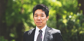
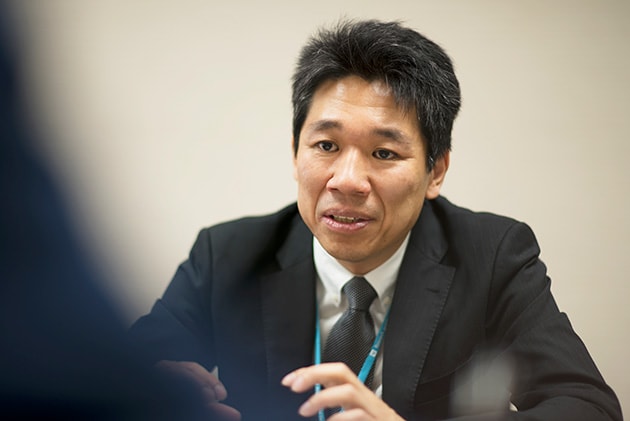
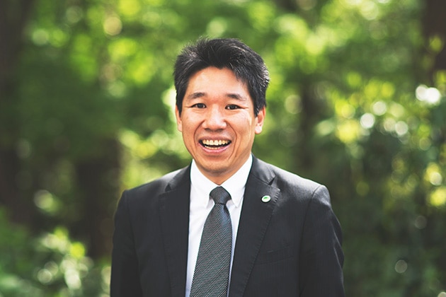
Masanao Yamaoka
Senior Researcher, Center for Technology Innovation - Electronics, Research & Development Group, Hitachi, Ltd.
1998: Graduated from Graduate School of Engineering at Kyoto University. Joined Hitachi Central Research Laboratory at Hitachi to engage in R&D into low power semiconductor digital circuits (low power memory circuits in particular).
2007: Received doctorate at Graduate School of Informatics, Kyoto University.
2010-2012: Participated in a joint IBM-Hitachi project at IBM Corporation.
2012-present day: Conducting R&D based on a new concept of computing technology. Currently leading Hitachi’s R&D into CMOS annealing machines.
Writer
Kenji Tsuda
International technology journalist, technology analyst
Kenji Tsuda is a freelance technology journalist who writes both in English and Japanese. With over 30 years of work experience covering the semiconductor industry, Tsuda has been offering various insights to the industry through his blog (newsandchips.com) and analytical articles. He is editor in chief of the Semiconportal site (www.semiconportal.com) and writes the “Car Electronics” article series for Mynavi News site as a columnist.
Tsuda started his career as a semiconductor device development engineer, before becoming a reporter for the Nikkei Electronics magazine at Nikkei McGraw-Hill (now Nikkei BP). At the company, he created several magazines including Nikkei Microdevices (in Japanese), Nikkei Electronics Asia, Electronic Business Japan, and Design News Japan (in English), and Semiconductor International Japanese Edition. Tsuda went freelance in June 2007 as an international technology journalist. Books he authored in Japanese include Megatrend in Semiconductors 2014-2023 (Nikkei BP), Why We Shouldn’t Let Go of the Semiconductor Industry (Nikkan Kogyo Shimbun, Ltd.), The Truth about the European Fabless Semiconductor Industry (Nikkan Kogyo Shimbun, Ltd.), The Latest Trends in Green Semiconductor Technology and New Businesses 2011 (Impress Corp.).
Contents
Cross Talk
Visiting Laboratories
Expert Interview
Topics
Report Series
- Motorization, Act II – The Age of Automated Driving

- How Society Will Change in the Digital Age
- Part 1
- What is Digitalization?

- Sports Technology Protecting Athletes and Providing Fairer Refereeing