


- Semiconductor Technology Now
Semiconductor Technology Now
Report Series
Part 1
The Race for 14 nm Semiconductor Fabrication to Intensify This Year Question: What Exactly Does the 14 nm Dimension Correspond to?
- February 27, 2015
Semiconductor technology has evolved in line with Moore’s Law until recently, with a single-minded focus on raising the integration level. The linewidth of the earliest integrated circuits (ICs) was 10 µm (1/100 mm) or so, whereas the latest technology has reached the level of 14 nm processing. At the same time, new transistor structures have introduced a three dimensional aspect, making it increasingly unclear what the 14 nm yardstick actually refers to. Part 1 of this report attempts to clarify the definition of minimum dimension. Part 2 will focus on the shift to 3D transistors, and Part 3 will examine the outlook of an extra-large wafer diameter (450 mm).
Recent tech news headlines often include references to 14 nm and 16 nm processes. “Intel to enter foundry business starting with 14 nm products,” “Samsung to license 14 nm process technology to American chip manufacturers,” and “TSMC to start risk production of 16 nm devices” are the cases in point. But what do the dimensions 14 nm and 16 nm actually refer to? One would imagine they refer to the minimum linewidth or minimum processing dimension, and it would have been a correct guess until a few years ago, but not anymore, because recent progress in chip scaling has made things a lot more complicated. What, then, do those dimensions correspond to?
Successive generations of ICs have achieved increasingly lower power consumption and faster processing speeds by reducing the linewidth and circuit size, thereby packing more transistors on a chip. As a result, the number of transistors on a chip has steadily increased in line with Moore’s law (a famous prediction that the number of transistors on a chip will double every 18-24 months). The minimum linewidth of the first-generation IC was 10 µm, which became narrower with each new process nodes (7µm, 5µm, 3µm, 2µm, 1.3µm, 1µm, 0.7µm, 0.5µm, 0.3µm, 0.2µm, 0.13µm), until the unit “µm” became inconvenient and was replaced by nm (1 nm=1/1000 µm). The minimum linewidth kept shrinking at the pace of approximately 0.7 times per process node, from 90 nm to 65 nm, 45 nm, 28 nm, and 20 nm, arriving at today‘s 16/14 nm node. Curiously, however, the minimum processing dimension of ICs in the latest 14 nm node is significantly shorter than 14 nm. In fact, the conventional notion of process node is losing its meaning.
Semiconductor scaling roadmap developed through global industry cooperation
In an effort to predict the trend in semiconductor scaling up to 15 years into the future, the Semiconductor Industry Association (SIA) is cooperating with semiconductor industry associations around the world, including the Japan Electronics and Information Technology Industries Association (JEITA). SIA compiles the results as the International Technology Roadmap for Semiconductors (ITRS), which is updated every year. Table 1 shows an excerpt of the roadmap technology characteristics table in the 2013 edition (released in April 2014).
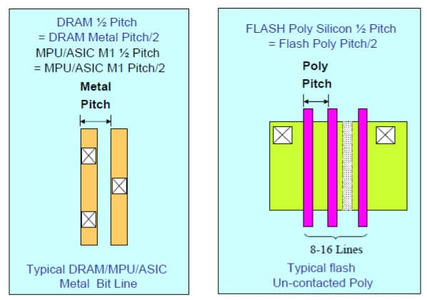
The ITRS uses the half pitch as a gauge of semiconductor scaling (Fig. 1). A pitch refers to the minimum center-to-center distance between interconnect lines. As the half pitch approximates the minimum linewidth, it has traditionally been used as an indicator of an IC’s integration level. In a dynamic random access memory (DRAM), half the pitch between metal lines in the lowermost interconnect layer (called Metal 1 or M1 layer) is used as a scaling indicator, also known as technology node (Fig. 1, left). In logic devices such as microprocessor units (MPUs) and application-specific integrated circuits (ASICs), too, the half pitch between Metal 1 lines is used as the indicator of the scaling level. In a flash memory device, the half pitch of the word lines (used for identifying individual memory cells in a matrix) serves as the scaling level indicator (Fig. 1, right). As the illustration shows, the lines of DRAMs, MPUs, and ASICs have contact holes in them for connecting the lines with the substrate or the upper layer, while the word lines in a flash memory device do not have any contact holes. For this reason, the half pitch of flash memory can be narrower than that of other devices, making the scaling level of flash memory more advanced than that of DRAMs.
While memory device manufacturers are adhering to the half pitch benchmark, the logic device industry led by Intel have departed from the ITRS guidelines, using instead the transistor gate length (the width of the green cuboid in the planar MOSFET on the left of Fig. 2) as the technology node indicator. Because recent advancements in process technologies have made it possible to make the actual gate length much smaller than that on the photomask (photosensitive glass plate for transferring the electronic circuit patterns on a silicon substrate), using gate length as the minimum processing dimension offers distinct advantages. It represents a new technology node, and its numerical value is far smaller than that of a half pitch node. Logic IC manufacturers and foundries have eagerly embraced gate length as a scaling indicator, because it allows them to boast their technological superiority, which is also good for business. Some people even call it a commercial node.
 |
Contents
Cross Talk
Visiting Laboratories
Expert Interview
Topics
Report Series

- Motorization, Act II – The Age of Automated Driving

- How Society Will Change in the Digital Age
- Part 1
- What is Digitalization?

- Sports Technology Protecting Athletes and Providing Fairer Refereeing