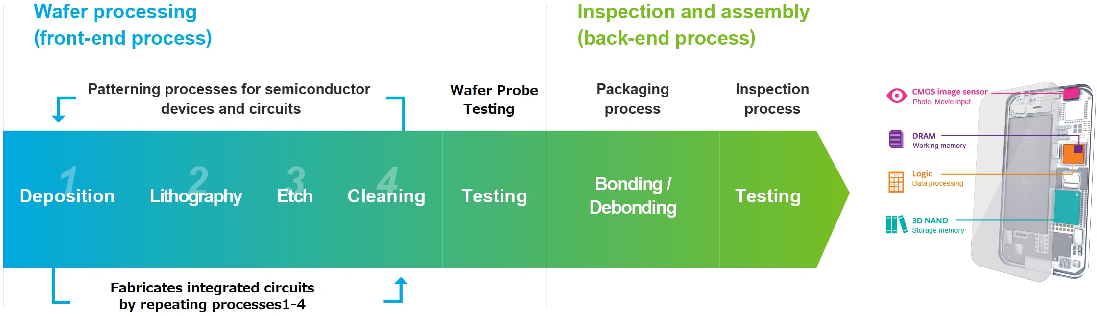
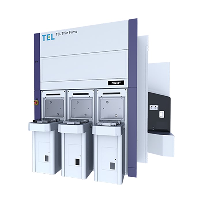
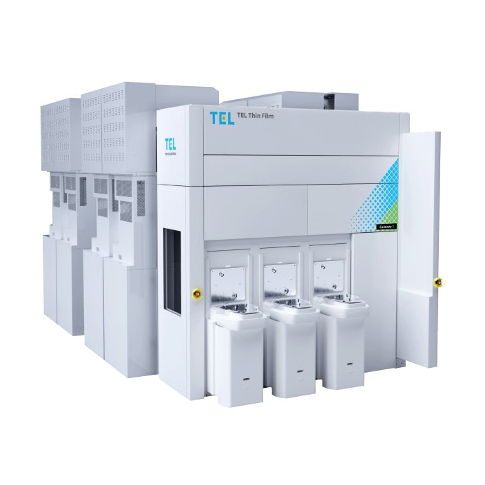
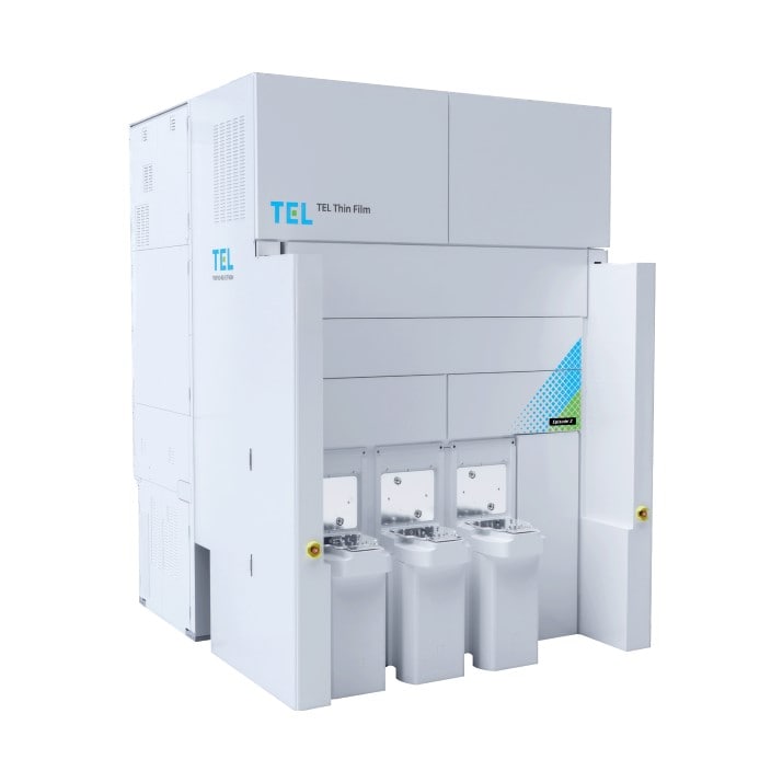
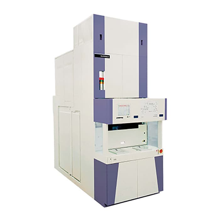
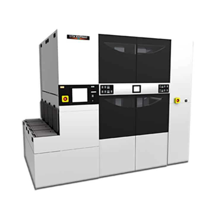
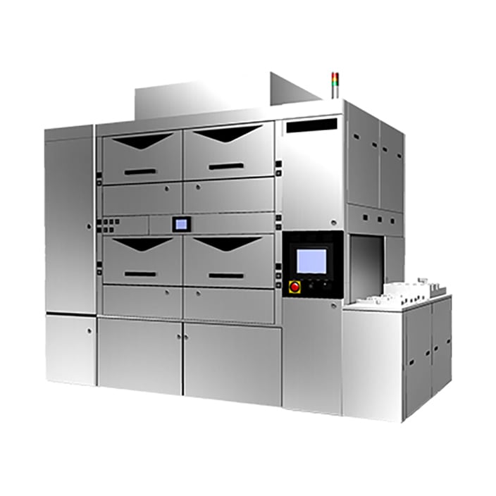
Deposition
Deposition is one of the important core processes in semiconductor manufacturing, in which dielectric or metal thin films are deposited on the wafer surface preparatory to forming device structures and wiring. Advanced technologies are required to deposit extremely thin films (1-10 nm thick) with excellent uniformity and to make highly etch-resistant films. TEL offers various types of deposition systems, including Oxide/Anneal (thermal deposition), CVD (chemical vapor deposition), ASFD (Advanced Sequential Flow Deposition), ALD (atomic layer deposition), and PVD (sputtering).
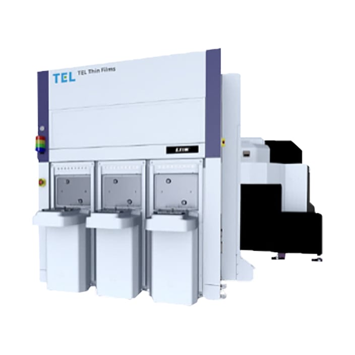
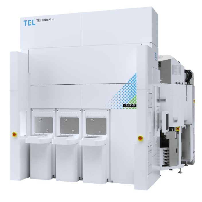
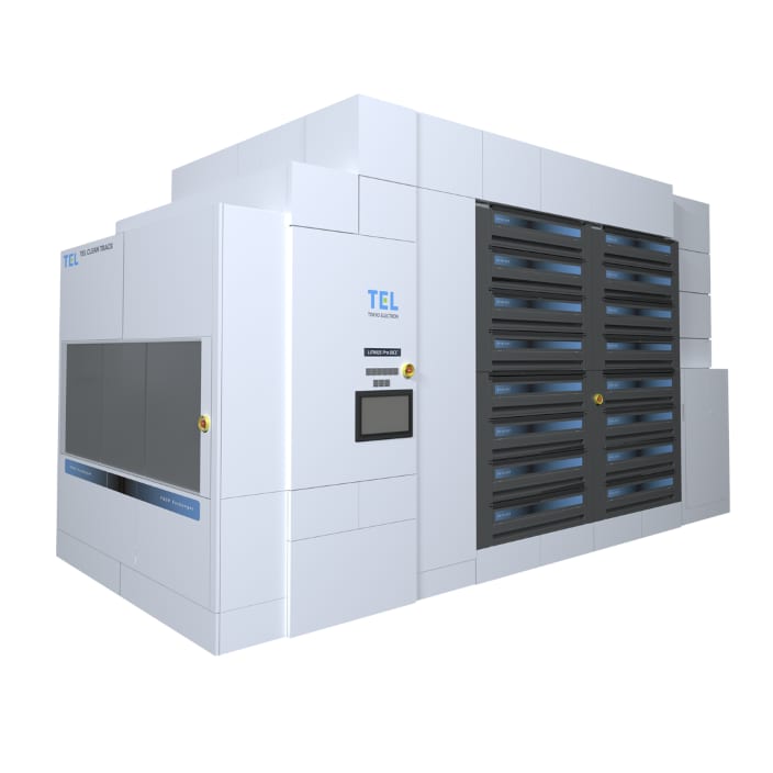
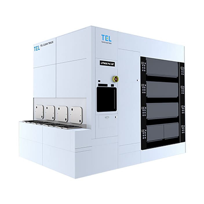
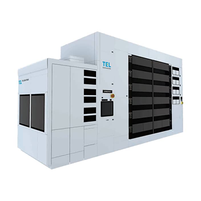
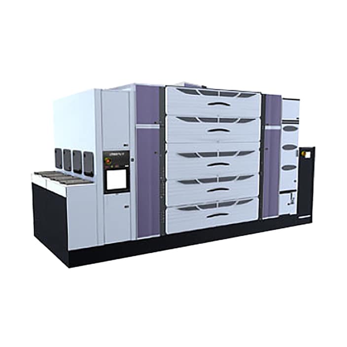
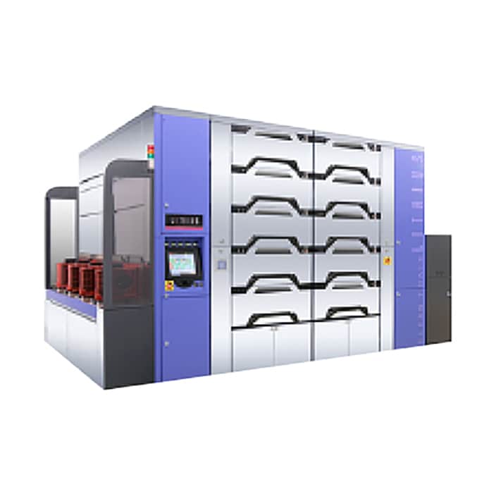
Lithography
Lithography is a core process of transferring extremely fine circuit patterns on wafer surfaces. The process to start by uniformly coating the photoresist on the wafer, expose the circuit pattern of the photomask on the coated photoresist by scanner. The photoresist is then selectively removed using a developer solution, leaving a circuit pattern on the wafer. The three steps of lithography (photoresist coating, exposure, and development) are often performed inline on an integrated system, which requires high reliability and precise control. TEL has 90% share of the overall in the Coater/Developer market and almost 100% share especially for the high NA process.
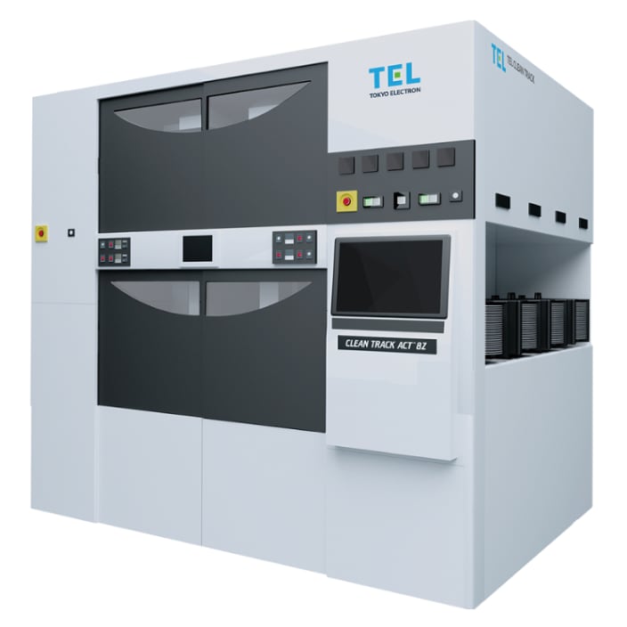
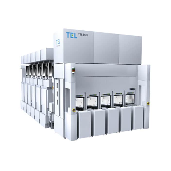
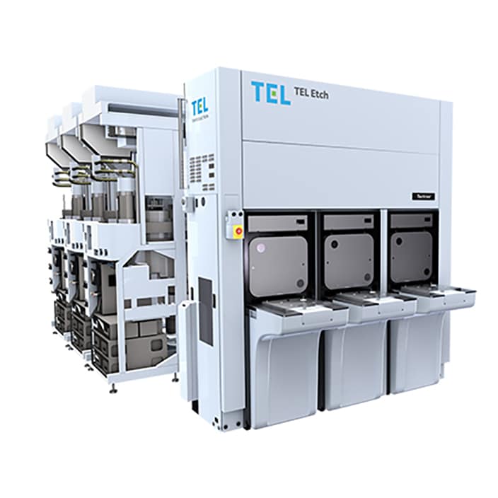
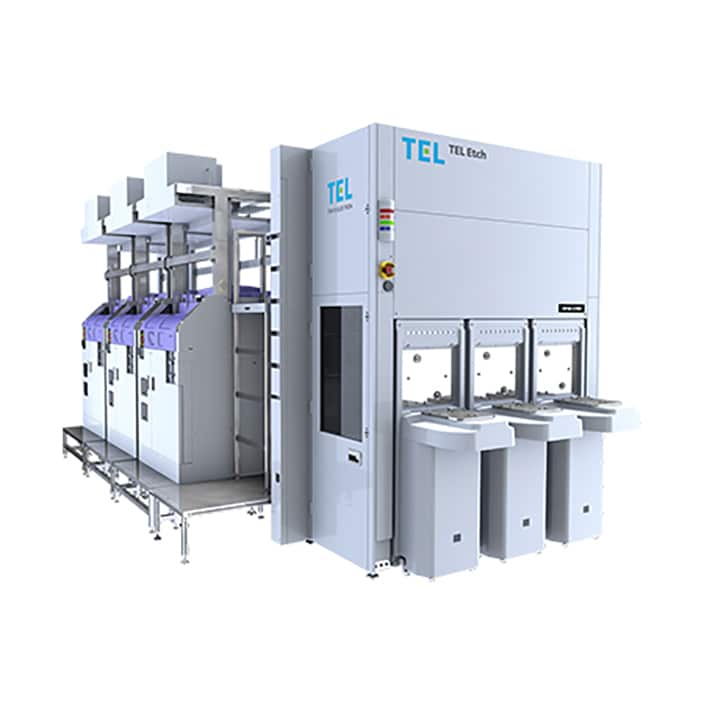
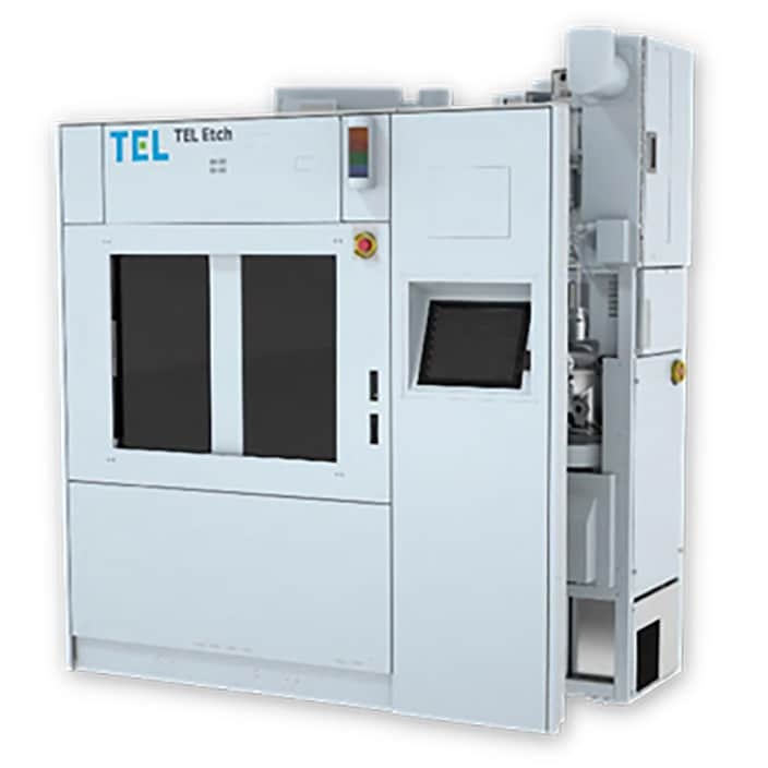
Etch
Etch is a critical process that defines minute circuit pattern formed by lithography on a thin film coated on a wafer. With the advancement of chip scaling, device structures of semiconductors are changing and new techniques have emerged including EUV lithography. Hence, new capabilities such as highly anisotropic etch and high selectivity between various films are required in etch systems. TEL has the second largest market share in dry etch systems. In particular, TEL excels in critical etch processes for advanced devices due to its distinctive technologies and superior competitive performance.
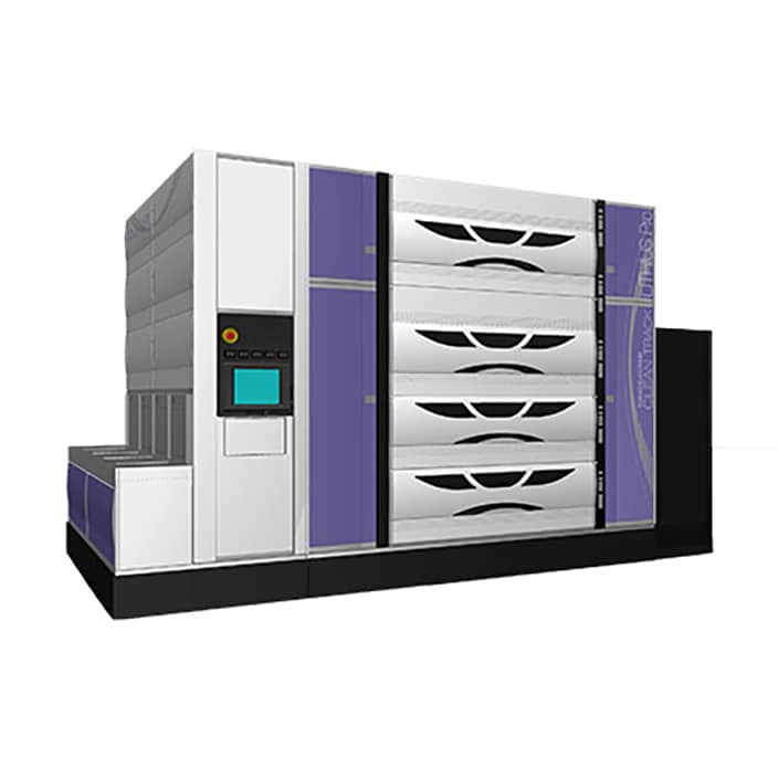
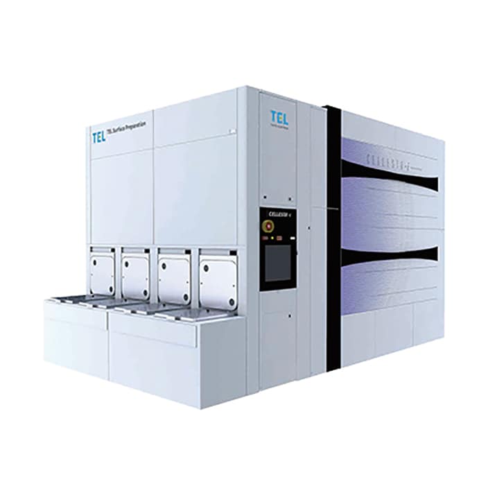
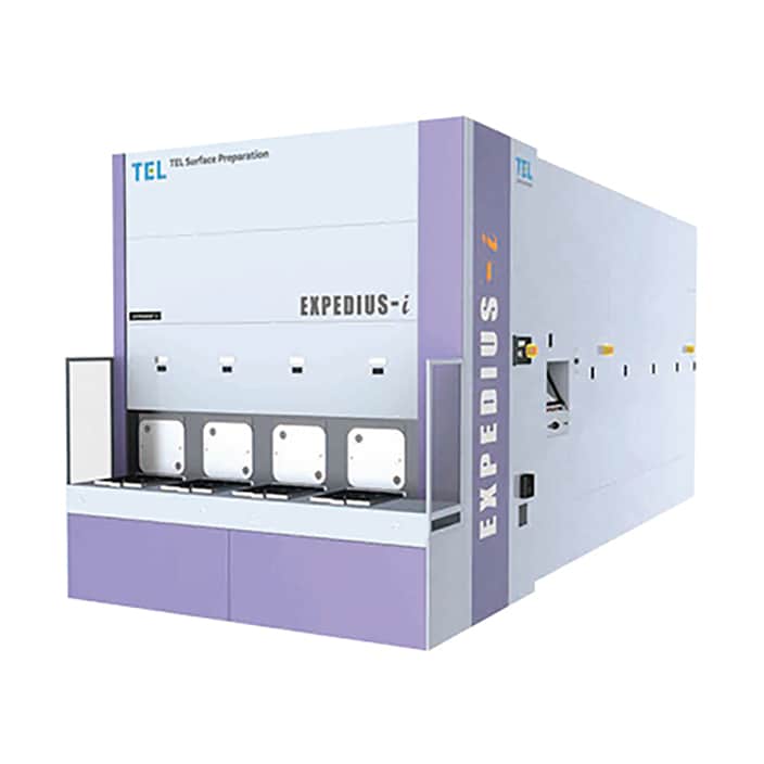
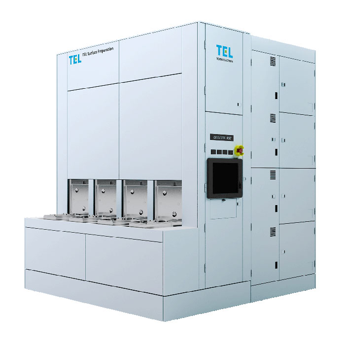
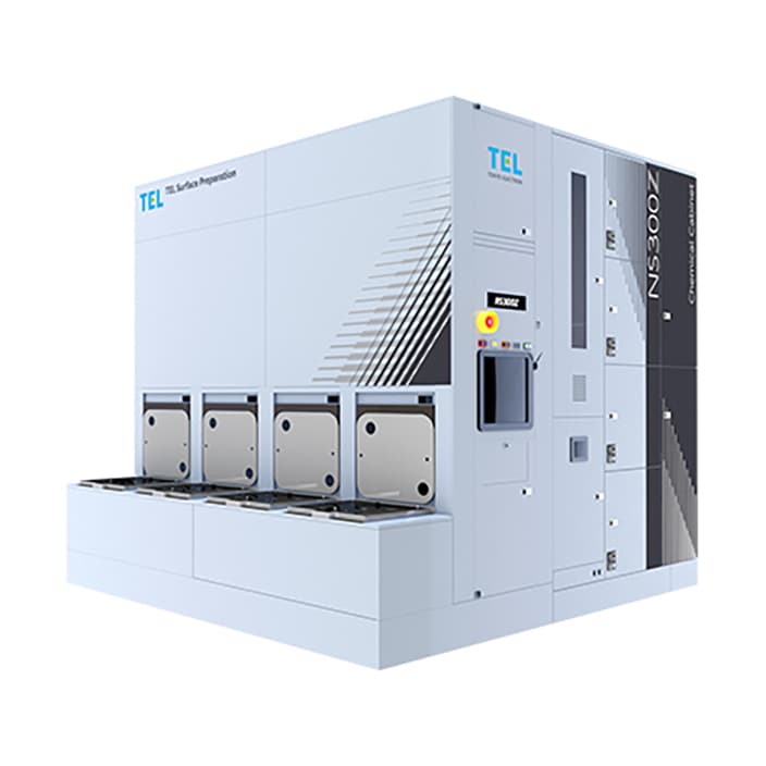
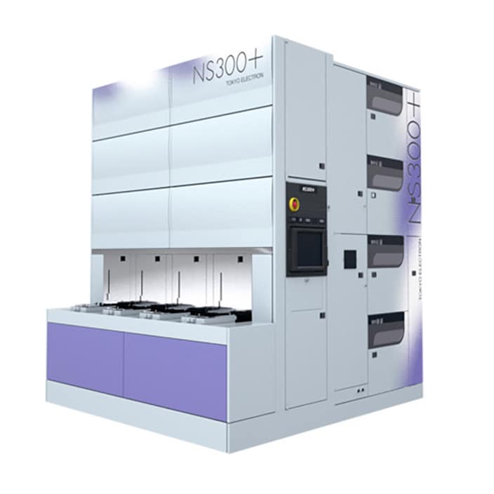
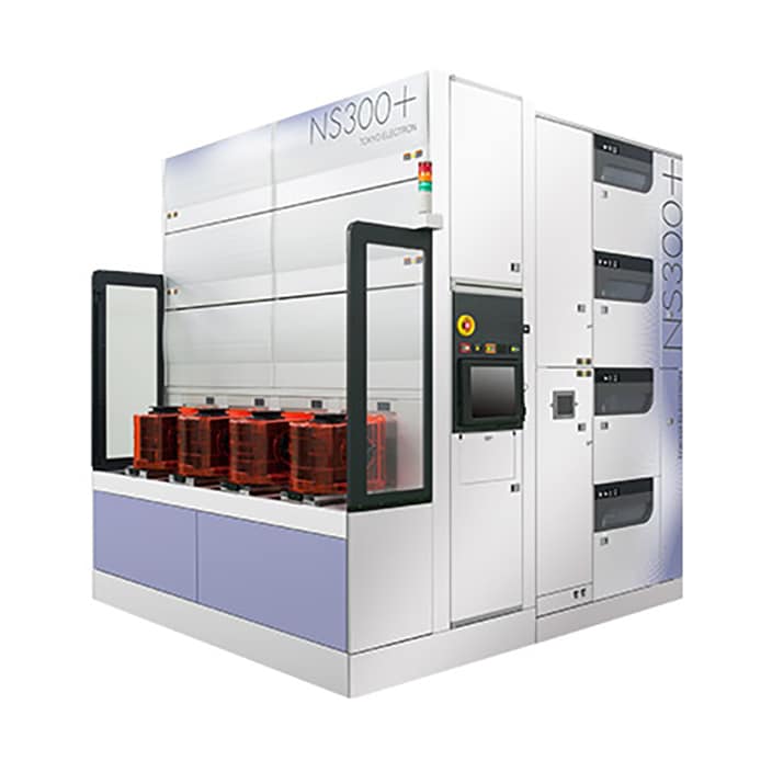
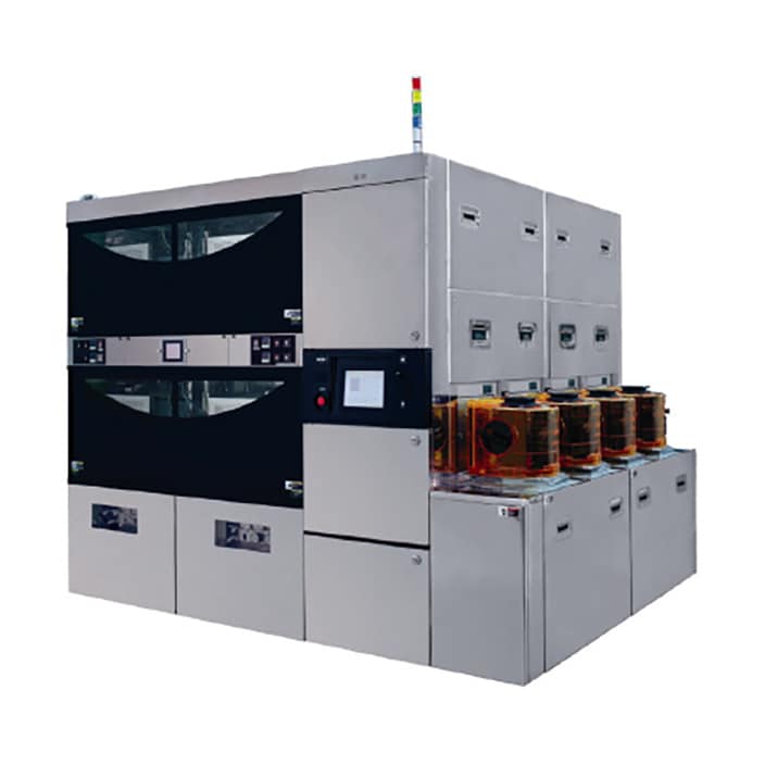
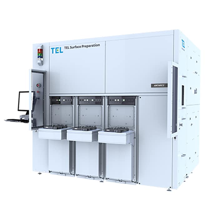
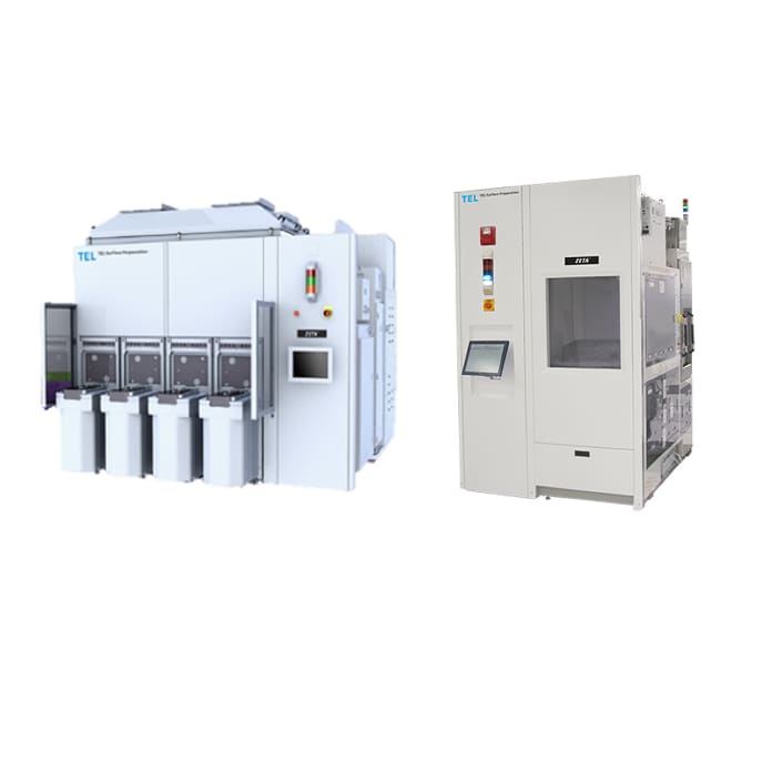
Cleaning
Cleaning is an essential step that must be performed between one process and another. Removing foreign objects from the circuit is vital to preventing defects, and drying is no less important than cleaning. TEL has the second largest share of wafer cleaning systems in the industry. Focusing on differentiating our critical processes and technologies for manufacturing the latest semiconductor devices, we are developing wafer cleaning technologies with outstanding process performance and productivity.
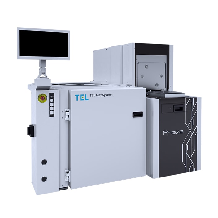
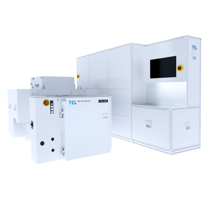
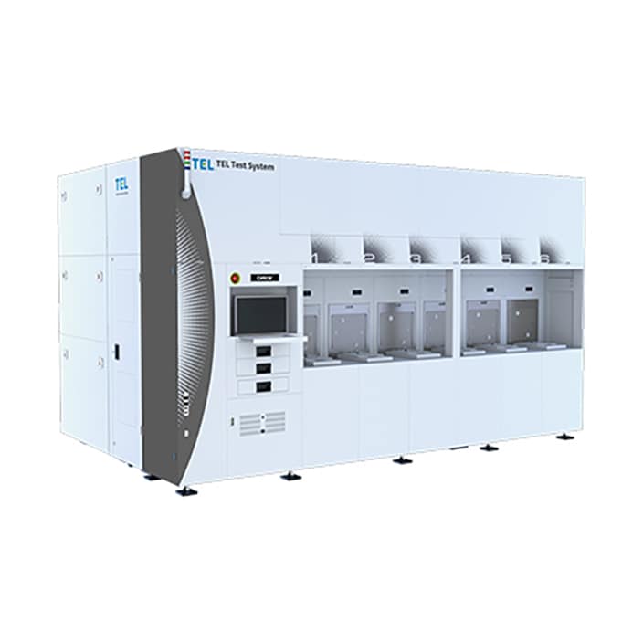
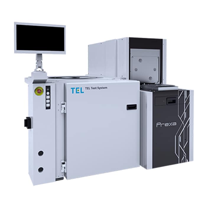
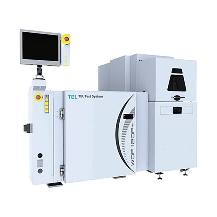
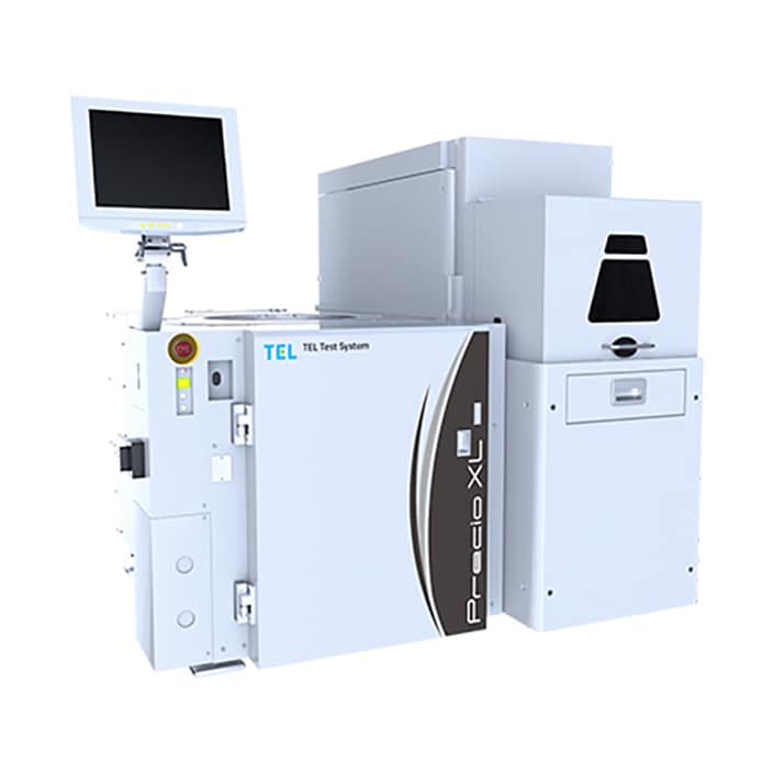
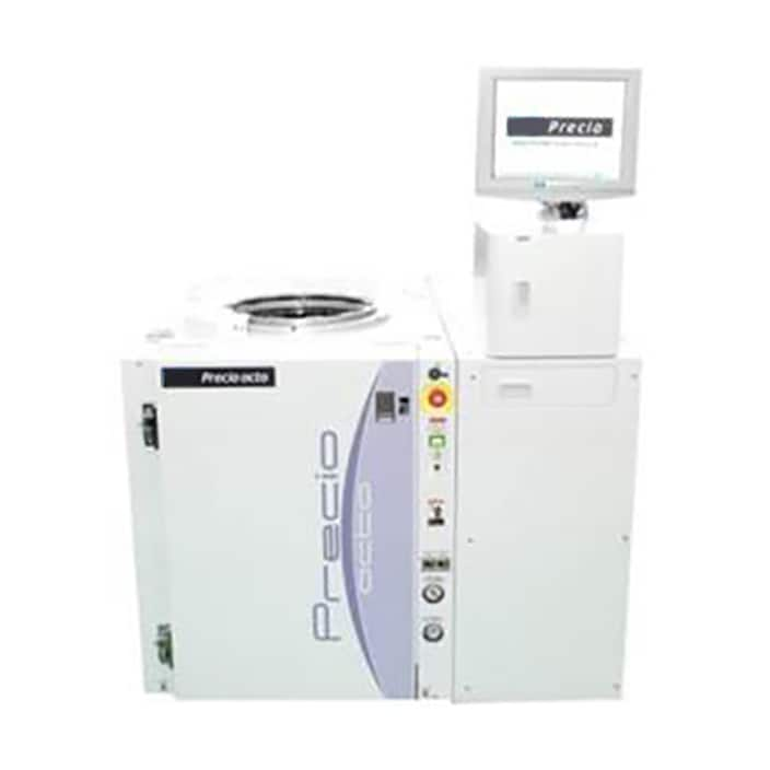
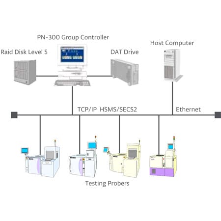
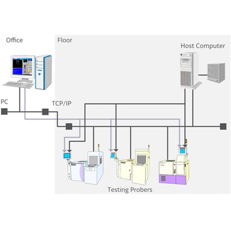
Test
With high performance of semiconductors, testing in production processes is becoming more important than ever. In the front-end process where circuits are formed on wafers, testing is performed to check if each process has been performed properly and to assure the quality of manufactured chips. TEL offers reliable solutions to satisfy the increasingly diverse technical requirements.
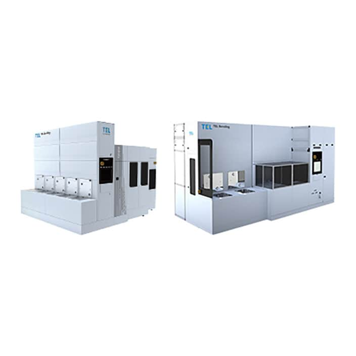
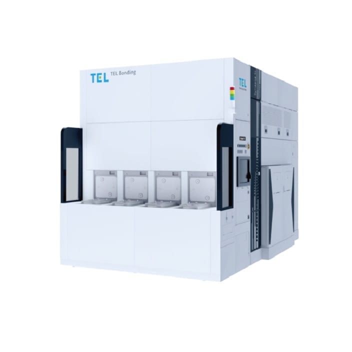
Bonding/Debonding
Introduction of 3D stacked devices is gaining momentum as further enhancement of semiconductor performance becomes necessary. One of the widely adopted techniques for implementing 3D stacking is wafer bonding. TEL integrates wide-ranging product technologies cultivated through its 60-year history to offer Wafer Bonding/Debonding systems and innovative eco-solutions that reduce the impact on the environment.