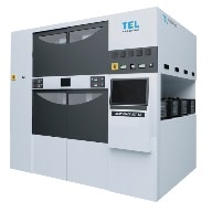
Coater/Developer ACT™ Series
Established position as an industry standard system

The CLEAN TRACK™ ACT™ Series was developed as coater/developer to support 300/200mm wafer processes, based on the technology from the CLEAN TRACK™ Mark Series. The key concepts are high throughput, footprint reduction, and up time improvement. Additionally, these technologies are also applicable to mask process and low-k dielectrics, besides photolithography. Thanks to its high reliability as an industry standard system, the ACT™ Series continues to contribute to the customers’ productions.
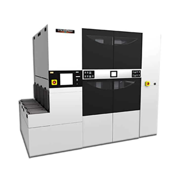
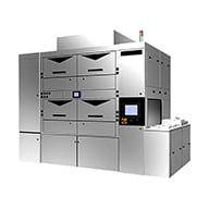
CLEAN TRACK™ ACT™ 12 is a Coater/Developer for 200/300mm wafers that offers stable, high-quality processing and enables a smooth transition from R&D to volume production. When used in-line with the exposure tool, the system is small in footprint and provides a high throughput due to its faster wafer transfer speed. The uptime has improved due to the increased reliability of components and ease of maintenance. The platform also uses a chemical filter and a high precision oven to support DUV processing.
CLEAN TRACK™ ACT™ 12 SOD is a spin-on dielectric system capable of coating, baking, and curing low-k dielectric films. It can process diverse SOD materials (including organic, inorganic, hybrid, and porous films) by using dedicated units optimized for respective materials. The system comes with a hotplate capable of high temperature processing in a low-oxygen environment, enabling in-line curing without using a conventional furnace.
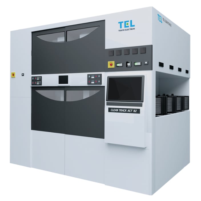
CLEAN TRACK™ ACT™ 8Z is a coater/developer for 75-200mm wafers. It was released in 2023 as a renewed version of CLEAN TRACK™ ACT™ 8, which had earned solid customer trust in the market. The system offers stable process performance and a smooth transition from R&D to volume production, as well as the capability to trace processes from CLEAN TRACK™ ACT™ 8. Additionally, back engineering from the latest 300mm systems has enabled a number of enhancements, significantly improving the system’s productivity and operability.
The system is also capable of spin-on dielectric (SOD) operations that include coating, baking, and curing of low-k dielectric films. It can process diverse SOD materials (including organic, inorganic, hybrid, and porous films) by using dedicated units optimized for respective materials. The system comes with a hotplate capable of high temperature processing in a low-oxygen environment, enabling in-line curing without using a conventional furnace.
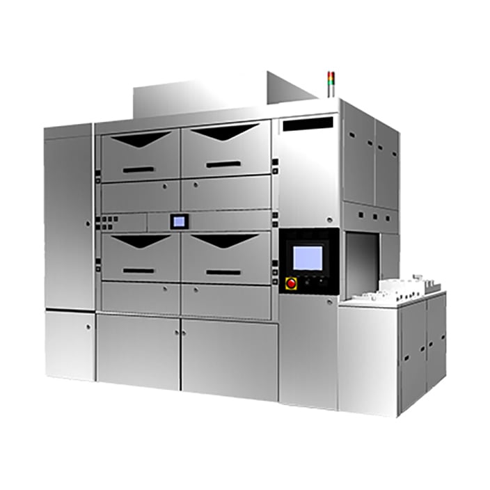
The CLEAN TRACK™ ACT™ M incorporates three separate high-performance application modules: photomask developer, resist coater, and PEB (Post-Exposure Bake) oven. The system provides sophisticated process control and techniques in the photomask manufacturing process to meet the advanced requirements from industry for OPC (Optical Proximity Correction), phase shifting, and the use of chemical amplification resists. The system extends TEL's long-standing semiconductor and FPD coating and developing technology, and achieves high reliability by adopting CLEAN TRACK™ ACT™ technology.
Product comparison
 ACT™ 12 SOD |
 |
 |
|
| Wafer size (mm) |
200,300 | 75 ~ 200 | 150 (6 inch MASK) |
| Availability | Certified used | New | New |
| Throughput (wph) |
Inline: 120 | Inline: 120 | S/A: 3 |
| Process | i-line, KrF, ArF, SOD/SOG, Pl | EB | |
| Substrates | Si, Glass | Si, GaAs, GaN, GaP, InP, SiC, Glass, Sapphire, AlTiC, LT, Thin & Thick |
6025 MASK |
| Additional features | Enclosed system, Precision hotplates | Enclosed system, Precision hotplates, Ingenio™ TL | Enclosed system |
CLEAN TRACK, CLEAN TRACK ACT, ACT, and Ingenio are registered trademarks or trademarks of Tokyo Electron Limited in Japan and/or other countries.
