

Discovery of "flowing crystal"
In 1888, Austrian botanist Friedrich Reinitzer at a plant physiology lab in Prague accidentally found that cholesteryl benzoate does not melt in the same manner as other compounds, but has two melting points.
The compound is solid at room temperature, but melts into a cloudy liquid when heated to a certain temperature, and melts again at an even higher temperature to become a clear liquid. Reinitzer asked German physicist Otto Lehmann to find out the working principle behind this phenomenon, who discovered that the compound in its cloudy liquid state has an optical property (anisotropy) observed in ordinary crystals. Since the liquid has a crystalline property, it was described as a flowing crystal. Afterward G.Friedel named it as liquid crystal. The discovery led to the wide use of liquid crystal in various kinds of displays and other applications.
Liquid crystal optical shutter
The orientation of the liquid crystal molecules changes easily as electric voltages and/or magnetic fields are applied, altering its transparency. This unique property of liquid crystal can be used to produce electronically controlled optical shutters. The liquid crystal used for this type of display device is known as twisted nematic (TN) liquid crystal. The TN liquid crystal molecules naturally form a twisted configuration, and when used in combination with polarization filters, the cell appears transparent. When a voltage is applied, however, the molecules untwist themselves, and the cell loses transparency. Displays based on this type of cells are known as TN displays, and laptops featuring improved TN displays was quite popular at one time.
However, it had serious disadvantages such as narrow viewing angle and poor color reproduction, and interest shifted to other types of liquid crystal displays (LCDs) that used transistors to improve performance.
Thin-film transistor revolutionizes the liquid crystal shutter
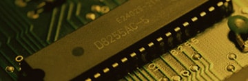
In 1975, amorphous silicon was discovered by Walter Eric Spear and others. Whereas crystalline silicon has the diamond cubic structure, in amorphous silicon the atoms are randomly bonded and loosely structured. Because the electrical and optical properties of amorphous silicon can be altered significantly depending on its composition and manufacturing process, the material played a critical role in the development of thin-film transistors (TFTs). Since TFTs can be produced under relatively low temperatures, it became possible to form LSIs directly on metal plates and glass panels, leading to the development of active matrix liquid crystal displays.
The use of TFTs dramatically improved the response of liquid crystal optical shutters, as well as the contrast and viewing angle of the display. Today, TFT is the most widely used technology for LCDs.
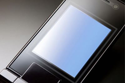
Rivalry among flat panel displays
Wall-mounted TV was once the stuff of dreams, but it is in every household today, thanks to the advancements in the flat panel display (FPD) technology.
While LCDs took an early lead in the FPD market, they were pursued by plasma displays, which use electrically charged ionized gases (plasmas) to release ultraviolet (UV) photons and light up phosphors. Other competing technologies have entered the fray lately, including organic electroluminescence (also known as organic light-emitting diode, or OLED) displays, and field emission displays (FEDs) that utilize cathode ray tube principles. Among these rivals, OLED displays seem to have the greatest potential for growth, and manufacturers are preparing for their mass production in Japan and elsewhere.